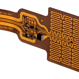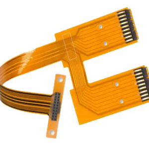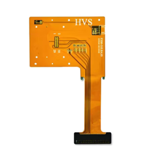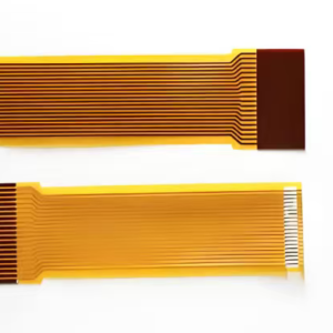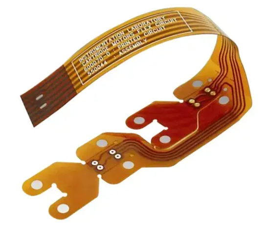
Custom High Precision Flexible PCB FPC with Stiffener, delivering precision-engineered polyimide flexible circuits reinforced with rigid stiffeners where needed. This design combines the flexibility and space savings of FPC with the mechanical support required for connectors and component mounting — ideal for medical devices, wearables, cameras, and other compact, high-reliability electronics.
Technical Specifications
| Item | Typical Value |
|---|---|
| Base Material | Polyimide (PI) 12.5–50μm |
| Layers | Single / Double / Multilayer FPC |
| Copper Type | RA (dynamic bend) / ED |
| Copper Thickness | 1/3–1 oz (12–35μm) |
| Stiffener | FR4 / PI / Stainless steel / PSA |
| Stiffener Thickness | 0.1–1.6 mm (per area) |
| Min Trace/Space | 3/3–2/2 mil |
| Min Hole Size | 0.1 mm (laser) |
| Impedance Control | 50/100Ω, ±10% (FPC) |
| Bend Radius | Dynamic ≥10× thickness; Static ≥3× |
| Operating Temp. | −65 ~ +150°C |
| Surface Finish | ENIG / Immersion Gold / OSP |
| Solder Mask / Coverlay | PI coverlay (flex) + LPI (stiffener area) |
| Precision Tolerance | ±0.05 mm (high-precision) |
Impedance Characteristics
– Controlled impedance (50/100Ω) with a tolerance of ±10% (FPC can be designed as microstrip or stripline).
– Use double-layer or multi-layer FPCs when a continuous reference ground plane is required.
– Bending areas may cause slight impedance variations; design margins should be incorporated.
– High-speed differential signaling (100Ω) is achievable on FPCs, provided that traces avoid areas subject to sharp or severe bending.
Signal & Electrical Performance
– Low dielectric constant (εr ≈ 3.3–3.5) with minimal signal loss.
– Suitable for medium-to-high-speed signals, low-level analog signals, and power connections.
– A continuous ground plane (in multi-layer designs) reduces crosstalk and improves shielding.
– Impedance control is limited in single-layer designs lacking a ground plane.
– High insulation resistance and excellent voltage withstand capability ensure electrical safety and reliability.
– Not suitable for ultra-high-frequency applications (use specialized high-frequency materials for such scenarios).
Manufacturing Advantages
– Stiffener Design: FR4, polyimide (PI), or steel stiffeners can be added to connector or mating areas to provide rigid support, while maintaining flexibility in the bending zones.
– High Precision: Tolerances for trace width, spacing, and hole positioning are within ±0.05mm, facilitating high-precision component mounting.
– Laser Drilling: Enables high-density interconnection via micro-vias (0.1mm).
– Rolled-Annealed (RA) Copper**: Offers superior durability for dynamic bending (capable of tens of thousands to 100,000+ cycles).
– PI Coverlay: Protects circuitry, with precise laser-ablated openings.
– 3D Assembly: Allows for folding and bending, reducing the need for additional connectors or wiring harnesses.
– Hybrid Assembly: Supports SMT component mounting on stiffened sections while retaining flexibility in the bending areas.