
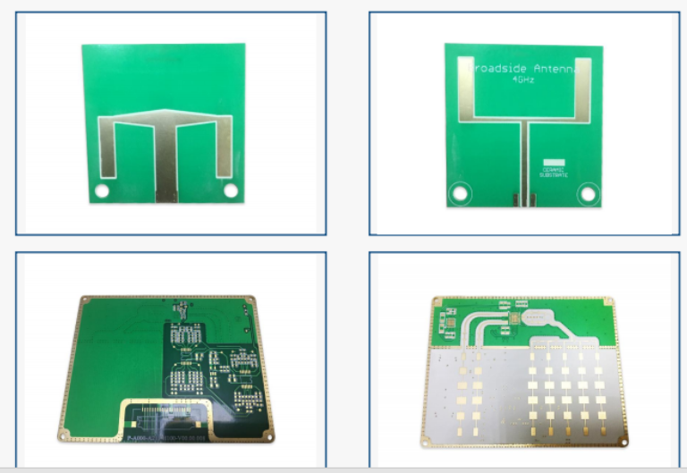
A high-frequency PCB is built differently from a standard board — the substrate itself affects signal quality.Standard FR-4 handles most circuit boards without issue. But when signals push into the high-frequency range — RF, radar, 5G, and fast digital interfaces — the board material itself starts to matter. At these frequencies, the substrate becomes part of the circuit, and the wrong material quietly destroys signal quality.
This guide explains what makes a high-frequency PCB different, which materials to choose, and the design rules that keep RF signals clean.
What Counts as “High Frequency”?
There is no hard line, but a few guidelines:
- RF and microwave— from hundreds of MHz up to tens of GHz
- High-speed digital— signals with very fast rise times, even at lower clock rates
- 5G, radar, satellite— frequencies from roughly 1 GHz upward
Above about 1 GHz, the properties of the substrate (not just the copper traces) begin to dominate signal behavior. That is when a high-frequency PCB material earns its place.
Why High-Frequency Materials Matter
At high frequencies, three material properties become critical:
| Property | What it controls |
| Dielectric constant (Dk) | Signal speed and impedance matching |
| Dissipation factor (Df) | Signal loss — lower Df means less attenuation |
| Consistency | Stable Dk across frequency and temperature, for predictable performance |
FR-4 has a relatively high and variable loss at high frequencies. Dedicated high-frequency laminates offer lower, more stable loss — at a higher material cost.
Common High-Frequency Materials
| Material | Typical use | Loss | Cost |
| PTFE (e.g. Rogers RT/duroid) | RF, microwave, antenna | Very low | High |
| Rogers / low-loss laminates | 5G, radar, high-speed digital | Low | Medium–high |
| High-Tg FR-4 / hybrid stacks | Moderately fast digital | Moderate | Low–medium |
| Hybrid (RF + FR-4 mixed) | Mixed designs on one board | Depends | Medium |
Hybrid boards combine a low-loss layer where the RF signals run with cheaper FR-4 elsewhere, balancing performance and cost.
Design Rules for High-Frequency PCBs
High-frequency design is stricter than standard digital design. The most important rules:
- Control impedance precisely.Match trace width, spacing, and stackup to the target impedance (typically 50 Ω single-ended, 100 Ω differential).
- Use a consistent ground plane.A solid, continuous reference plane under the RF traces controls impedance and reduces interference.
- Keep RF traces short and direct.Long, meandering traces add loss and unwanted coupling.
- Manage vias carefully.Via stubs and impedance mismatches at transitions degrade RF signals — use back-drilling or avoid vias where possible.
- Watch the stackup.Layer count and material choice together determine the achievable impedance and isolation.
How Layer Count and Materials Combine
Your layer count decision directly affects a high-frequency stackup. More layers give room for dedicated ground planes and controlled impedance routing, but they also add cost. For RF boards, the balance between material, layer count, and stackup must be settled early in design — mistakes are expensive to fix later.
When Do You Actually Need a High-Frequency PCB?
You need dedicated high-frequency materials when:
- Signals run above roughly 1 GHz
- You need tight, repeatable impedance control
- Signal lossover the trace length matters
- The design targets RF, microwave, radar, 5G, or high-speed dataapplications
For simple boards with low-speed signals, standard FR-4 remains the right, cost-effective choice.
Get Help With Your High-Frequency Stackup
Designing a high-frequency PCB correctly requires matching material, layer count, and stackup to your performance targets. A wrong choice shows up as poor signal integrity — and it is costly to redesign.
At Volectronics Tech Co., Ltd, we work with high-frequency laminates and can review your stackup and layer count before production, so your RF design performs the way you intend.Discuss your high-frequency PCB stackup →