
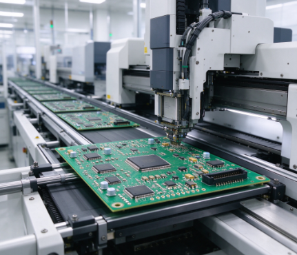
How does a bare copper-clad laminate become the finished PCB inside your product? The process looks simple on a schematic, but behind every board are dozens of precise manufacturing steps — each one affecting quality, yield, and cost.
This guide walks through the complete PCB manufacturing process, from raw laminate to a board ready for component assembly. Understanding these steps helps you design better boards, avoid DFM issues, and know exactly what you are paying for.
Step 1: Preparing the Raw Laminate (Copper-Clad Laminate)
Every PCB starts as a copper-clad laminate (CCL) — a fiberglass substrate with copper foil laminated on one or both sides. The base material’s grade (such as FR-4) and the copper thickness define the board’s electrical and mechanical properties from the start.
The laminate is cleaned and inspected before imaging, because any surface contamination or defect will be carried through every later step.
Step 2: Inner Layer Imaging and Etching
For multilayer boards, the inner layers are printed first. A photosensitive film (photoresist) is applied, then the circuit pattern is transferred by exposing it through a film or laser imager. UV light hardens the photoresist where the circuit should remain.
The board is then etched, removing the unwanted copper. The remaining copper forms the traces and pads. After etching, the photoresist is stripped away, leaving a clean copper pattern.
Step 3: Layer Alignment and Lamination
The inner layers are aligned and stacked with insulating prepreg sheets between them, then pressed together under heat and high pressure. This bonds the layers into a single multilayer board.
Alignment accuracy is critical here — misregistered layers cause via-to-pad errors that fail later. This is why a DFM review of your stackup before production matters.
Step 4: Drilling
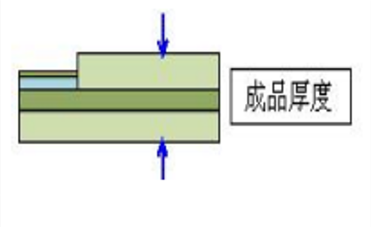
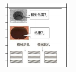
Holes are drilled for vias and through-hole components. Drilling is done with precision CNC machines, and for high-density boards, laser drilling creates the smallest microvias.
Drill quality affects the plating and final reliability. Hole size, position, and cleanliness all matter — and this is where your layer count and via design decisions come into play.
Step 5: Plating and Copper Deposition
The drilled holes are plated with copper to create conductive connections between layers. An electroless copper deposit first coats the hole walls, then electrolytic plating builds up the copper thickness.
This step electrically connects the layers through the vias, turning the drilled holes into working interconnections.
Step 6: Outer Layer Imaging and Etching
The outer layers are imaged and etched the same way as the inner layers, forming the final trace pattern on the board surfaces.
Step 7: Solder Mask
A solder mask is applied over the board, leaving openings only where components will be soldered. The mask protects the copper from oxidation and prevents solder bridges between closely spaced pads.
The solder mask color (commonly green) is applied and cured, with the pads precisely opened for assembly.
Step 8: Silkscreen
The silkscreen layer prints reference designators, logos, and labels onto the board. It helps assembly technicians and future repairs identify components and orientation.
Silkscreen must not overlap pads or exposed copper — a common DFM check point.
Step 9: Surface Finish
A surface finish is applied to the exposed pads to keep them solderable and protect the copper from oxidation. Common finishes include HASL, ENIG, and OSP, each balancing cost, shelf life, and solderability.
The right finish depends on your application, assembly method, and product lifetime — which is why it deserves its own careful selection.
Step 10: Electrical Testing
Before the board ships, electrical testing verifies that the circuits are correct — checking for opens, shorts, and proper connectivity. Automated testers probe the board against the netlist to catch manufacturing defects.
Step 11: Profile and Final Inspection
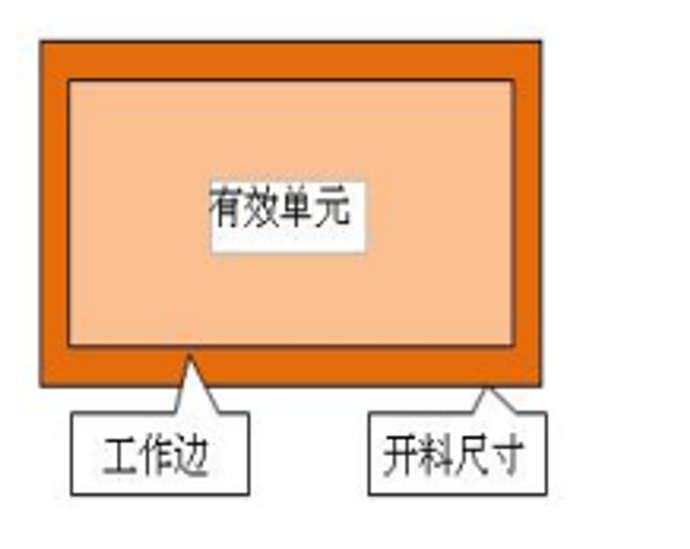
The board outline is routed or v-cut to separate individual boards from the panel, and a final visual and quality inspection checks the finished product before it is packed for assembly.
From Bare PCB to Assembly
The finished bare board is now ready for the next stage: component assembly — where solder paste, placement, and reflow turn the empty board into a working PCBA. Each step above directly affects how smoothly that assembly runs and how reliable the final product is.
Why the PCB Manufacturing Process Matters to You
Knowing these steps helps you:
Design with manufacturability in mind (via types, layer count, clearance)
Choose the right base material and surface finish
Set realistic expectations for cost and lead time
Catch potential issues before they become expensive rework
At Volectronics Tech Co., Ltd, we control every step of this process — from laminate selection and inner-layer imaging through drilling, plating, and final test — with continuous quality checks along the line.Discuss your PCB manufacturing requirements →