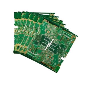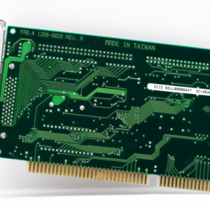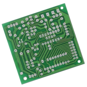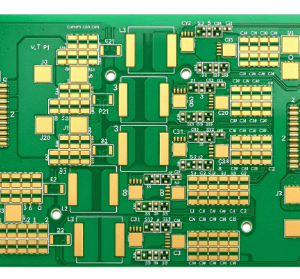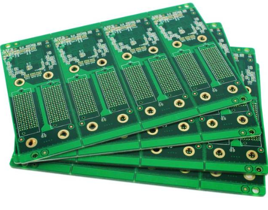
Multilayers FR4 PCB with Matrix Pin Holes, Custom Layers is a custom multi-layer test matrix PCB built on FR4 material, widely used for pogo pin test fixtures, burn-in boards and signal adapter modules.
I. Specifications
| Item | Specification |
|---|---|
| Board Type | Multilayers FR4 PCB with Matrix Pin Holes, Custom Layer Count |
| Base Material | FR-4, TG130 / TG150 / TG170 / TG180 high Tg FR4 optional |
| Layer Count | 4 / 6 / 8 / 10 / 12 layers, custom layers supported |
| Copper Foil | 1oz(35μm), 2oz(70μm), 3oz(105μm), heavy copper available |
| Pin Hole Pitch | 2.54mm / 1.27mm / 1.0mm / custom matrix pitch |
| Finished Pin Hole Size | 0.4mm ~ 2.0mm, match spring test pins / pogo pins / connector pins |
| Pad for Pin Hole | Anti-pull reinforced pad, annular ring ≥0.15mm |
| Solder Mask | Green / Black / Blue / Red LPI solder mask; mask defined or non-mask defined |
| Silkscreen | White legend, matrix coordinate marking (X-Y grid numbering) |
| Surface Finish | ENIG, ENEPIG, OSP, HASL, Immersion Silver, Hard Gold Plating (for frequent pin contact) |
| Board Thickness | 1.0mm ~ 3.2mm, customizable |
| Min Line / Space | 0.075mm / 0.075mm |
| Impedance Control | ±10%, ±5%, single-ended & differential impedance available |
| Operating Temperature | -40℃ ~ +130℃ (depends on FR4 Tg grade) |
| Insulation Resistance | ≥ 10¹² Ω·cm |
| Withstand Voltage | AC 500V~1500V (depends on interlayer dielectric thickness) |
| Tolerance | Outline ±0.1mm, hole position tolerance ±0.05mm |
| Certification | IPC-6012, RoHS, REACH |
II. Features
- Standard or custom matrix pin hole array, compatible with pogo pins, spring test probes, pin sockets and press-fit pins.
- Multi-layer stack-up design, separate power layers, ground layers and signal layers inside the board.
- High Tg FR4 substrate with excellent dimensional stability, less expansion under repeated pin insertion and temperature cycling.
- X-Y coordinate silkscreen marking for each matrix hole, convenient for debugging, wiring mapping and fixture assembly.
- Support heavy copper design for high-current power distribution inside the matrix board.
- Optional hard gold plating on pin pads, greatly improve wear resistance for thousands of contact cycles.
- Custom layer stack-up, impedance simulation, cross-ground shielding for high-speed differential signals.
- Suitable for test fixtures, interface adapter boards, burn-in boards, industrial matrix switching modules.
III. Design Principle
- Matrix pin hole array:Holes are arranged in regular X-Y matrix grid. Each hole serves as an independent signal/power access point for test pins or connectors.
- Multilayer stack-up separation:Internal layers are divided into signal layer, GND plane, PWR plane. Ground planes provide shielding and stable reference potential for signals routed between matrix holes.
- Annular ring & pad reinforcement:Larger annular ring around pin holes to resist mechanical stress from repeated pin pressing-in and pulling-out, prevent pad lifting.
- Via design strategy:Use buried vias / blind vias optionally to route signals from top matrix pins to inner/bottom layers without occupying surface space.
- Coordinate grid system:Silkscreen X/Y labels map every pin position, so engineers can quickly locate each signal channel.
Core difference vs normal protoboard:This is a multi-layer internal routing matrix board, not just empty grid holes; signals can be pre-routed inside different layers.
IV. Signal & Electrical Performance
- Insulation & isolation:FR4 dielectric provides high insulation resistance between adjacent matrix channels, low crosstalk for multi-channel parallel test signals.
- Impedance & high-speed signal:With complete GND reference plane inside stack-up, it supports controlled impedance signals such as LVDS, USB, Ethernet for test fixture signal transmission.
- Current carrying capacity:Inner heavy copper layers can distribute large current for power matrix channels; track width and copper thickness are calculated according to current requirement.
- Contact resistance:ENEPIG / hard gold finish keeps stable low contact resistance; HASL/OSP is for low-cycle, low-cost prototype use only.
- Crosstalk suppression:Complete ground plane between signal layers reduces crosstalk among dense matrix channels, critical for multi-channel synchronous testing.
- Limitation:Not suitable for ultra-high frequency RF unless special stack-up and low Dk material are specified.
V. Core Manufacturing Advantages
- High-precision CNC drilling for matrix pin holes, tight hole position tolerance ±0.05mm, guarantee smooth insertion of pogo pins.
- Reinforced pad process for pin holes, anti-lifting, anti-crack under long-term repeated pin contact.
- Controlled lamination process for multi-layer FR4, low internal stress, stable dimension, avoid hole position shift after pressing.
- Optional hard gold plating on pin contact pads: wear-resistant, low contact resistance for mass production test cycles.
- Flexible custom stack-up: adjust dielectric thickness, copper weight, layer sequence according to impedance and current demand.
- 100% AOI + electrical open-short test; sampling pin insertion test for fixture-grade orders.
- Support panelization, large-format matrix board for big test jigs.