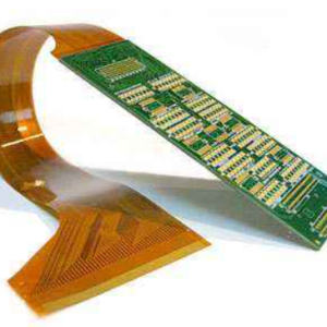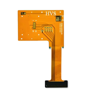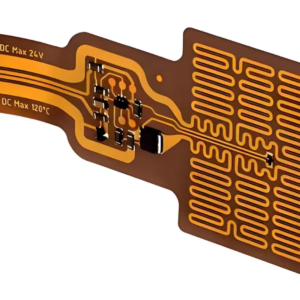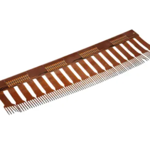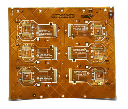
Polyimide(PI) Flex PCB with Gold Finger is a high-performance flexible printed circuit built on polyimide substrate. It features gold finger plating on the connector edge, delivering excellent bending resistance, high temperature stability and reliable plug-in connectivity. Widely used for dynamic bending and high-reliability interconnection applications.
Specifications
- Substrate: Polyimide (PI), 12.5μm / 25μm / 50μm / 75μm thickness
- Copper foil: Rolled annealed copper (RA Copper), 9μm / 12μm / 18μm / 35μm
- Layers: 1-layer, 2-layer, multi-layer flexible PCB
- Solder mask: PI coverlay (yellow/black), optional liquid photoimageable solder mask (LPI)
- Gold Finger: Hard gold plating; Gold thickness: 0.05μm ~ 1.0μm, Nickel underlayer 2~5μm
- Minimum line width/space: 0.075mm / 0.075mm
- Minimum hole size: 0.1mm (laser drilling)
- Bend cycles: ≥100,000 times (depends on copper thickness & design)
- Operating temperature range: -200℃ ~ +260℃
- Surface finish (non-gold finger area): ENIG, Immersion Silver, OSP
Impedance Characteristics
- Controlled impedance available: 50Ω, 75Ω, 90Ω, 100Ω differential impedance
- PI material has stable dielectric constant (Dk ~3.2~3.5 at high frequency), low Df loss
- PI substrate maintains consistent dielectric property under repeated bending, minimal impedance drift
- Impedance tolerance: ±10% standard, ±5% for high precision requirement.
- Critical notes: Trace width, substrate thickness, coverlay thickness must be strictly controlled for impedance matching; gold finger region usually no impedance control, designed for contact conduction
Design Principle
- PI Substrate Selection: Polyimide is chosen for its outstanding flexibility and thermal resistance, suitable for repeated folding, bending, dynamic movement.
- Gold Finger Area Design: Edge connector pads are separated from circuit traces; gold finger region is designed for physical mating & plugging. Hard gold prevents wear and oxidation during repeated insertion/extraction.
- Copper Trace Layout: Traces in bending zones are placed at neutral axis, rounded corners instead of sharp angles to avoid copper crack under flexing.
- Coverlay Protection: Coverlay covers most circuit area, only expose gold fingers and component pads, isolate circuit from dust, moisture and mechanical scratch.
- Stiffener Option: Add PI/FR4 stiffener underneath gold finger section to support plug force, prevent flex PCB deformation during connector mating.
Manufacturing Advantages
- Hard Gold Plating on Fingers: Hard gold with nickel barrier layer, anti-wear, anti-oxidation, stable contact resistance for thousands of plug cycles.
- PI Material Superiority: High heat resistance, can withstand reflow soldering without delamination, suitable for SMT assembly.
- Precision Laser Processing: Laser drilling & coverlay opening for fine line and small feature on flexible board.
- Custom Stiffener Integration: Stiffener bonded under gold finger area to strengthen connector part, easy assembly.
- High Flex Durability: Rolled annealed copper + PI stack, support frequent dynamic bending.
- Strict Electrical Test: Continuity, insulation resistance and impedance test before shipment.
Application Scenarios
- Consumer electronics: Foldable screen modules, camera modules, laptop internal connectors
- Medical devices: Minimally invasive medical probes, wearable medical sensors
- Automotive electronics: On-board flexible wiring, vehicle display connection
- Industrial control: Robotics moving joint wiring, industrial sensor interconnection
- Aerospace: Lightweight flexible interconnection components
- Optical communication: Optical module internal flexible link
VolectronicsTech Co., Ltd was established in 2017 and is dedicated to providing one -stop services for orders ranging fromprototyping and small-to-medium batch production to large-scale mass production.
We offer a diverse selection of PCB material, including FR4, Rogers, Metal based, TU, Isola, PI, and other high-frequency material, providing a wide range of options to meet your specific requirements.Welcome to contact us!