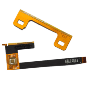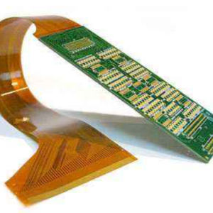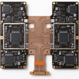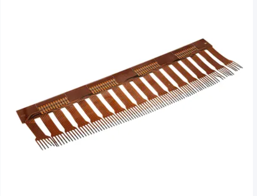
Flexible PCB, also known as FPC, is a polyimide-based flexible circuit widely used for sensors, image detectors and display modules. Our custom fine pitch long tab flexible PCB adopts adhesiveless PI and RA rolled copper to achieve high wiring density, stable high-speed signal transmission and reliable repeated bending performance.
1. Specification Table
| Item | Standard Capability | Custom Advanced Option | Remarks |
|---|---|---|---|
| Layer Count | 1L / 2L | 4L (rare for dynamic bending zones) | 1L/2L adhesiveless CCL is mainstream for sensors & displays |
| PI Base Film Thickness | 12.5μm / 25μm | 10μm ~ 50μm | Dk≈3.4~3.6 @1GHz, low water absorption, high heat resistance |
| Copper Foil Type | RA Rolled Annealed Copper | ED Electrodeposited Copper (optional) | RA copper delivers far better bending life; mandatory for dynamic flexing |
| Finished Copper Thickness | 12μm (0.33oz), 18μm (0.5oz) | 9μm / 35μm | 9~12μm thin copper preferred for fine pitch; 35μm for high current |
| Min Line / Space | 40μm / 40μm | 25μm / 25μm | Core fine pitch spec; Long Tab finger pitch: 0.3mm / 0.2mm / 0.15mm |
| Min Laser Via Diameter | Φ0.1mm | Φ0.075mm | HDI blind vias, keep away from bending areas |
| Overall FPC Thickness | 0.08~0.18mm | Down to 0.06mm ultra-thin version | Excludes stiffener |
| Long Tab Length | 5~50mm | Custom >100mm available | Stiffener (FR4/SUS/PI) on Tab for bonding & plugging strength |
| Stiffener Material | FR4 / PI | SUS Stainless Steel, PSA adhesive backing | Stiffener only on Tab/finger area; no hard material on flex zone |
| Surface Finish | Immersion Ni/Au | Hard electroplated gold, OSP, carbon ink, tin plating | Immersion Au / hard gold preferred for display/sensor fingers for low contact resistance |
| Operating Temperature | -40℃ ~ +125℃ | -55℃ ~ +150℃ | PI base; peak 260℃ for 10s (SMT reflow compatible) |
| Minimum Bend Radius | Static: 6 × total thickness; Dynamic: 10 × total thickness | Special ultra-thin PI down to 5 × thickness | Complies with IPC-2223; No vias, pads or stiffeners in bending zones |
| Impedance Control | Single-ended 50Ω, Differential 100Ω | Tolerance ±10%; premium ±5% | Designed for MIPI DSI/CSI differential pairs for display & image sensors |
| Dimensional Tolerance | ±0.1mm (≤100mm) | ±0.05mm precision grade | Critical to control stretch & thermal deformation for long Tab FPC |
| Coverlay | 12.5μm PI coverlay (acrylic adhesive) | Black light-blocking coverlay (OD≥4.0) | Black coverlay for optical sensors / OLED to block stray light interference |
2. Performance Characteristics
- Ultra-fine Pitch High Density Wiring 25μm class L/S with 0.15–0.3mm finger pitch, supporting COF, driver IC, pixel sensor arrays and multi-channel touch acquisition routing. High channel count within narrow width to reduce stack thickness.
- Structural Advantage of Long Tab Stiffened Tab region provides bonding / connector strength while the middle section retains full flexibility. It bridges sensors installed inside optical cavities and driver PCBs on main boards. Symmetric stack and low-CTE PI are adopted to mitigate impedance drift and tensile deformation on long strips.
- Excellent Repeated Bending Reliability RA rolled copper + adhesiveless PI substrate achieves 50,000 ~ 500,000 dynamic bending cycles. Suitable for foldable displays, wearable sensors and hinge modules. Neutral-axis routing design prevents copper fatigue cracking.
- Low Dielectric & Low Loss High-frequency Performance Low Dk/Df PI supports MIPI CSI/DSI, LVDS high-speed image signals for CMOS image sensors and display drivers.
- Optical Compatibility for Sensors Optional black light-shielding coverlay with OD≥4.0 blocks visible stray light and suppresses light crosstalk and dark current noise. Transparent PI version is available for light-transmissive touch sensors.
- Long-term Environmental Stability Low moisture absorption, resistant to cleaning chemicals, stable through thermal cycling (-40~125℃, 1000 cycles, resistance drift <10%). Resists ion migration under 85℃/85%RH, suitable for automotive, industrial sensors and outdoor displays.
- Lightweight & 3D Conformability Thin flexible substrate can be folded, wrapped around hinges and attached to curved surfaces for narrow-bezel, under-display and tight stacking applications.
3. Design Principle
Core target: Combine ultra-fine high-density routing, stable impedance, bending reliability and optical isolation (for sensors) on a long extended Tab structure.
- Symmetric Stack-up Design Adhesiveless 2L CCL is preferred. Balanced PI/copper layers offset internal thermal stress and suppress warpage and dimensional shift of long Tab FPC. Asymmetric adhesive stacks easily cause S-shaped twisting.
- Neutral Axis Bending Control Conductors are placed near the neutral plane in bending zones. Vias, pads and solid copper planes are forbidden in flex regions. Ground planes use mesh copper (≈60% coverage) to retain impedance performance while reducing stiffness.
- Fine Pitch Routing Rules Teardrops are added at trace-to-pad transitions to relieve stress concentration. Differential pairs are length-matched, parallel and with constant spacing to minimize skew and crosstalk over long Tab transmission paths. Uniform dielectric thickness maintains consistent impedance along the whole Tab.
- Zoned Long Tab Architecture
- Tab finger zone: Stiffener + thick gold for ZIF/BTB connector or COF thermal bonding
- Middle flex segment: Non-stiffened flexible area for bending and strain compensation
- Sensor pad zone: Local coverlay opening for chip or pixel array bonding
- Anti-interference Optical Design Black PI coverlay is applied underneath optical sensor channels. Signal traces are routed away from light-sensitive areas to reduce reflective leakage and optical noise.
- DFM Compensation Layout scaling pre-compensation is applied to offset stretch from exposure, etching and lamination, guaranteeing accurate pitch at the distal end of the long Tab.
4. Solder Mask / Coverlay Properties
Liquid solder mask is rarely used on standard FPC. PI coverlay acts as the solder mask and protective layer for this fine-pitch long Tab display & sensor product.
- Standard Amber Transparent PI Coverlay (Acrylic Adhesive) Thickness: 12.5μm PI film plus adhesive layer. Withstands 260℃ reflow. Provides insulation, oxidation protection and short-circuit prevention. Limitation: transparent, may introduce stray light interference for optical sensors.
- Black Light-blocking Coverlay (Preferred for Sensors & Displays) Optical density OD≥4.0 for high visible light blocking (400–700nm). IR-transparent variant available for infrared sensors. Heat-resistant and flex-compatible with standard PI processes. Note: Black fillers slightly increase Dk; impedance simulation must be re-calibrated for high-speed MIPI signals.
- Liquid Photoimageable PI Solder Mask (High-end COF only) Higher resolution down to 20μm fine openings, low modulus and bendable. High cost and strict yield control, only adopted for premium COF driver FPC, not common for general long Tab FPC.
Key coverlay performance indicators: Peel strength ≥0.8N/mm, no blistering under soldering heat, chemical resistance, no ion migration under humidity, no adhesive bleeding at fine circuit edges (critical for fine pitch yield).
5. Core Manufacturing Advantages
- Adhesiveless Substrate Process Eliminates adhesive flow and adhesive aging compared with adhesive-based FPC. Better thermal stability, lower Df, longer bending life and consistent impedance over long Tab lengths. Standard for high-end displays and image sensors.
- Laser Imaging & HDI Laser Drilling Laser direct imaging achieves 25μm L/S ultra-fine circuits. Laser microvias avoid offset and stretching issues seen with mechanical drilling on thin long flex circuits.
- Segmented Lamination & Precision Dimensional Compensation Dynamic stretch compensation for long Tab FPC during exposure, etching and lamination to guarantee accurate finger pitch at the far end and prevent bonding misalignment.
- Zoned Stiffener Lamination Stiffener is bonded only on Tab bonding zones, leaving the main flex section pure PI. Precision lamination does not introduce stress defects in bending areas.
- Black Coverlay Light-shield Lamination Bubble-free bonding with tight edge bleed control to eliminate stray light hotspots on optical sensors.
- Inline Impedance & Electrical Full Inspection Continuous impedance testing for differential pairs, continuity, isolation and high-voltage test to screen hidden open circuits and out-of-spec impedance caused by long transmission paths.
- Laser Profiling Laser cutting reduces copper tearing and cracking at fine-pitch edges compared with mechanical punching.
6. Signal & Electrical Performance
Suitable for MIPI DSI/CSI, LVDS, I2C, SPI and low-level analog sensor acquisition signals (imaging, photoelectric, pressure sensing).
- Impedance Control Differential 100Ω ±5%~±10% (MIPI standard), single-ended 50Ω. Impedance gradient from variable dielectric thickness and trace width on long Tab is tightly controlled to avoid signal reflection and closed eye diagrams.
- Insertion Loss / High-frequency Attenuation Low-Df PI keeps attenuation acceptable at 1–2GHz. Longer Tab increases loss; smooth RA copper and low-loss PI are recommended for extra-long versions.
- Crosstalk Fine pitch creates tight trace spacing. Differential isolation, ground shielding or mesh ground design is implemented to reduce adjacent channel crosstalk, which is critical for weak analog sensor signals.
- DC Resistance Thin copper on long Tab introduces voltage drop. Trace resistance must be calculated for analog sensor channels; 18μm / 35μm copper is preferred for longer signal runs.
- Insulation Performance Insulation resistance ≥10⁹Ω @ 500V DC. No electrical migration under 85℃/85%RH, preventing micro-leakage that causes sensor noise and drift.
- Differential Skew Length matching for differential pairs controls intra-pair timing offset for stable sampling of high-speed image data.
- ESD Performance Optional extra shielding ground layer provides ESD protection for photoelectric and CMOS sensors to reduce electrostatic damage risk.
7. Typical Applications
CMOS image sensor FPC, under-display optical fingerprint sensors, OLED/LCD display driver COF extension cables, touch array sensors, miniature spectrum sensors, AR optical modules, foldable hinge display flex cables.
If you need, I can make a concise web product description version optimized for your PCB/FPC independent store.