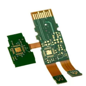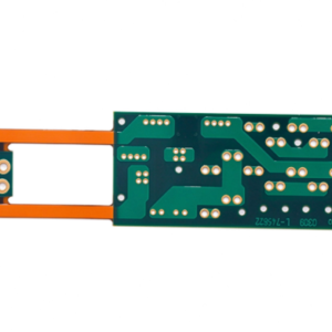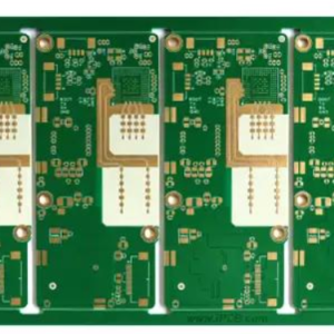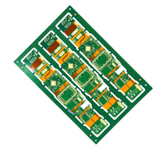
Rigid Flex PCB combines rigid FR4 sections and flexible PI polyimide substrate, widely used for devices requiring folding, bending and compact packaging.
Our Rigid Flex PCB adopts reliable blind and buried via structures to achieve high-density interconnection within limited space. Different copper thickness options are available to meet your current-carrying and impedance control requirements. Volectronics Tech Co., Ltd provides custom rigid flex PCB fabrication and one-stop PCBA assembly service for consumer electronics, industrial control and security systems.
Specifications
- Substrate: Rigid part – FR4; Flexible part – Polyimide (PI), 12.5μm / 25μm / 50μm
- Copper Foil: RA Rolled Annealed Copper 9μm /12μm /18μm /35μm
- Stackup: Multi-layer rigid-flex structure
- Via Type: Blind vias, buried vias + optional through vias
- Min Blind Via Diameter: 0.1mm (laser ablation)
- Min Buried Via Hole: 0.15mm
- Min Line Width / Space: 0.075mm / 0.075mm
- Coverlay for Flex Area: PI coverlay, thickness 12.5μm /25μm
- Stiffener: Optional PI / FR4 stiffener for connector mounting zone
- Surface Finish: ENIG, Immersion Silver, OSP, Hard Gold (for gold finger optional)
- Operating Temperature: -40℃ ~ +260℃
- Bend Cycles: ≥100,000 times (design & copper thickness dependent)
Performance Characteristics
- Hybrid Mechanical Performance: Rigid FR4 zones support component soldering and assembly; PI flex zones enable repeated folding & dynamic bending.
- High Density Interconnection: Blind and buried vias route signals internally between layers, saving board space, reducing board footprint.
- Thermal Stability: PI flex material maintains stable property under thermal cycling, low thermal expansion, less risk of delamination.
- Vibration & Shock Resistance: Reduces separate cable connectors, fewer solder joints, improves reliability in moving/vibration environments.
- 3D Assembly Capability: Can fold into 3D shape to fit confined device housing.
Design Principle
- Dual Material Stack-up: Separate rigid FR4 regions for heavy component placement; PI flexible regions reserved for bending movement.
- Blind & Buried Vias Design Logic
- Blind via: Connects outer layer to inner layer only, does not penetrate entire board stackup
- Buried via: Interconnects inner layers only, completely hidden inside stack, no opening on outer surface
- Flex Zone Layout Rules: Traces in bending area placed at neutral axis; rounded trace corners, avoid sharp angles to prevent copper cracking during flexing.
- Transition Zone Management: Optimize rigid-flex transition area, reduce stress concentration between FR4 and PI boundary.
- Layer Planning: Assign high-speed signals on inner layers, use buried vias for inner layer interconnection to shorten signal path.
Solder Mask Properties
- Rigid area: LPI liquid photoimageable solder mask (green/black/red optional)
- Flex PI area: PI coverlay (main protection), optional LPI solder mask for flex section
- Adhesion: Strong bonding on FR4 and PI substrate, no peeling during repeated bending and SMT reflow
- Heat Resistance: Tolerate lead-free reflow up to 260°C, no blistering, delamination
- Insulation & Protection: Block moisture, dust, oxidation; prevent short circuit between adjacent traces.
- Note: Coverlay is the primary protective layer for PI flex area, different from rigid board solder mask.
Signal & Electrical Performance
- Controlled Impedance: Support 50Ω single-ended, 90Ω /100Ω differential impedance; tolerance ±10% standard, ±5% available
- Dielectric Property: PI Dk ~3.2~3.5, low Df, stable dielectric constant under bending and temperature variation
- Insulation Resistance: ≥10⁹ Ω @ DC 500V
- Withstand Voltage: ≥1.5kV AC
- Signal Advantage: Blind & buried vias shorten signal path, reduce parasitic inductance and crosstalk, suitable for high-speed signals
- Current capacity: Determined by copper weight and trace width
- Electrical Test: 100% continuity and isolation test after fabrication
Application Scenarios
Medical endoscopic devices, aerospace modules, foldable consumer electronics, industrial robotic moving joints, optical communication modules, automotive compact sensing units.