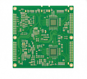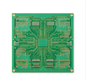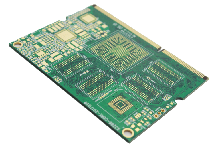
This 10-layer High TG HDI PCB board adopts immersion gold surface finish and gold finger design, built with high TG substrate material to withstand high operating temperature and thermal cycling shock. The HDI stacked microvia structure enables dense circuit routing, suitable for compact high-performance electronic modules.
High TG base material prevents delamination and resin cracking during repeated reflow soldering, critical for industrial and high-reliability applications. Immersion gold (ENIG) delivers flat pad surface, excellent oxidation resistance and stable solderability. The precision gold fingers are manufactured with controlled thickness for stable plug-and-unplug connection, low contact resistance and long service cycles.
Our 10L HDI PCB supports fine line width/spacing, small laser drilled microvias and controlled impedance requirements. It is widely used in industrial control, smart home hardware, security electronics and consumer high-end devices.
Specifications
| Item | Typical Value |
|---|---|
| Layers | 10 layers |
| HDI Level | 1st/2nd order, blind/buried via |
| Material | High Tg FR4 (170°C+) |
| Microvia | 0.075–0.15 mm laser, aspect ≤1:1 |
| Via Filling | Copper plug / resin plug |
| Min Trace/Space | 3/3–2/2 mil |
| Min Hole Size | 0.1 mm laser; 0.2 mm mechanical |
| Copper Thickness | 1 oz |
| Board Thickness | 1.0–2.4 mm |
| Surface Finish | Immersion Gold (ENIG) |
| Gold Finger | Edge connectors, beveled, ENIG |
| Impedance Control | 50/100Ω, ±10% |
| Solder Mask | Green/Black LPI |
| UL Rating | UL 94V-0 |
Impedance
- 50/100Ω precision control (±10%).
- Microstrip/stripline impedance control; matched differential pair lengths.
- Solid power/ground plane references for stable impedance.
- Impedance matching design in the gold finger area to ensure consistent connector contact impedance.
Signal Performance
- Micropores have short paths, small parasitic effects, and low high-speed losses.
- Low-loss materials are available to improve signal integrity.
- Complete ground plane shielding, low crosstalk, low EMI.
- Suitable for high-speed digital, communications, servers, and AI interconnection.
- The gold finger is reliable for plugging and unplugging, with stable contact and wear resistance.
Manufacturing Advantages
- High Tg: Resists thermal stress from multiple reflow cycles and prevents thermal deformation.
- Micro-via Build-up: Sequential build-up of blind/buried vias; supports high routing density.
- Copper-filled Plating: Supports via-in-pad designs; ensures high density and reliability.
- Gold Finger Beveling: Beveled edge contacts ensure smooth insertion/extraction and reliable connectivity.
- ENIG (Electroless Nickel/Immersion Gold) Finish: Flat and coplanar surface; excellent solderability and long shelf life.
- Impedance Control: Symmetrical stack-up and precise trace widths ensure signal consistency.
Volectronics Tech Co., Ltd is a professional PCB & PCBA manufacturer based in Shenzhen, China, supplying high-quality PCB and PCBA to clients worldwide.
We offer a diverse selection of PCB material, including FR4, Rogers, Metal based, TU, Isola, PI, and other high-frequency material, providing a wide range of options to meet your specific requirements.Welcome to contact us!