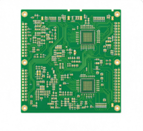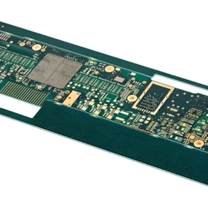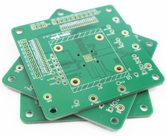
High Speed Controlled Impedance HDI Multilayer PCB adopts high-performance low Dk/Df substrate material, HDI microvia technology, precise impedance control design. It is built for high-speed digital transmission scenarios, ensures stable signal integrity, widely used in data communication, server, optical module, high-end industrial control and automotive electronics.
Specifications
- Layers: 4~20 layers, customizable
- Base Material: FR-4 high TG / low loss FR4, optional high-speed substrate (Isola, Rogers, Panasonic)
- Copper Thickness: 0.5oz ~ 2oz
- Min Line Width/Spacing: 0.075mm / 0.075mm
- Min Microvia Diameter: 0.1mm (blind & buried vias)
- Board Thickness: 0.4mm ~ 3.2mm
- Surface Finish: ENIG, HASL, OSP, Hard Gold, Immersion Silver
- Solder Mask: Green, Black, Blue, White, Matte/Gloss available
- Tolerance of Dimension: ±0.1mm
- Impedance Tolerance: ±5% (standard), ±3% for strict requirement
- TG Value: 170℃ / 180℃ / 210℃ optional
Impedance Characteristics
- Supports single-ended impedance & differential pair impedance design (50Ω, 100Ω, 90Ω, 85Ω etc., customized)
- Pre-stack impedance simulation before production, adjust dielectric thickness, trace width, copper thickness to meet target impedance
- Tight impedance tolerance ±3%~±5%, reduce impedance discontinuity caused by microvia, trace necking
- Low dielectric loss (Df), stable Dk over wide frequency range, minimal impedance shift at high frequency
- Impedance testing by TDR (Time Domain Reflectometer) for verification before shipment
Signal & Electrical Performance
- Low insertion loss & low return loss, excellent signal integrity for high-speed signals up to 25Gbps+
- Controlled crosstalk between adjacent differential pairs, reduce electromagnetic interference (EMI)
- Low parasitic capacitance and inductance, minimize signal reflection & distortion
- Insulation resistance: ≥10¹² Ω, Dielectric Withstanding Voltage ≥500V
- Excellent tracking resistance, stable electrical performance under continuous high-frequency operation
- Optimized return path design to reduce ground bounce and noise
Manufacturing & Process Advantages
- HDI Microvia technology (laser drilling blind/buried vias): higher routing density, save board space, shorten signal path length
- Pre-production stack-up simulation + DFM review, catch impedance and SI risk at early design phase
- Precise inner layer lamination & dielectric thickness control, guarantee consistent impedance across whole panel
- Fine line & fine spacing process capability, support dense BGA pad routing
- Strict layer registration control, prevent layer misalignment affecting impedance and yield
- Full inspection: AOI, X-ray, TDR impedance test, continuity & isolation electrical test
- Custom stack-up, impedance value and material selection to match customer high-speed design requirement
Typical Applications
Servers, network switches, optical transceivers, high-speed storage, 5G communication modules, high-end industrial controllers, medical imaging equipment, automotive radar electronics.