Product Overview
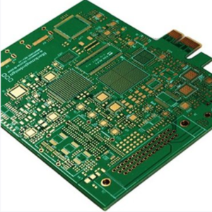
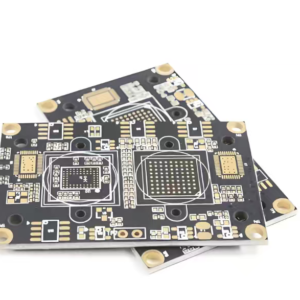
HDI High Density BGA Test Fixture PCB with Symmetric Routing is a high-density interposer test board specially built for BGA chip verification, ICT/FCT test jigs and probe station applications.
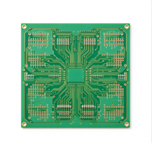
It adopts HDI microvia stack-up, fine trace technology and fully symmetric differential routing layout. Symmetric routing ensures equal trace length, consistent impedance and matched signal delay on differential pairs and multi-channel parallel signals.
It connects BGA pads to test probe points, test pins or edge connectors, eliminating skew and crosstalk during high-speed chip testing. Widely used as the core carrier of semiconductor test fixtures, SOC, FPGA, DDR and high-speed transceiver verification platforms.
Core Advantages
- Strict symmetric & length-matched routing Differential pairs and multi-bus traces are routed symmetrically, precisely controlled trace length matching, minimize signal skew, guarantee synchronous sampling during high-speed BGA testing.
- HDI high-density structure for fine-pitch BGA Support microvias, stacked vias, blind & buried vias, adapt 0.4mm / 0.5mm / 0.65mm fine pitch BGA pads, breakout routing without pad damage.
- Stable controlled impedance performance Controlled single-ended / differential impedance (50Ω, 90Ω, 100Ω etc.), tight impedance tolerance, reduce reflection and signal distortion in test path.
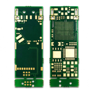
- Optimized for test fixture & probe contact Gold-plated probe landing pads with smooth surface, high hardness gold plating, anti-wear for repeated probe contact thousands of times; pad size and anti-solder dam design match spring probe requirements.
- Low crosstalk & clean reference plane Complete solid ground/power plane, isolation shielding between test channels; symmetric layout reduces electromagnetic interference between adjacent BGA channels.
- High repeatability for mass testing Uniform stack-up, stable material, consistent electrical performance board to board; suitable for continuous production ATE test, not only laboratory prototype verification.
- Custom BGA breakout & pin assignment Support custom BGA pin map reallocation, fan-out from BGA array to orderly test pin matrix, convenient fixture assembly and debugging.
Technical Parameters
| Item | Specification |
|---|---|
| Product Name | HDI High Density BGA Test Fixture PCB with Symmetric Routing |
| Stack-up Type | HDI, blind / buried / stacked microvia structure (2+n+2, 4+n+4 etc.) |
| Base Material | FR-4 High Tg / Mid-loss high-speed material (Isola, Shengyi, Rogers hybrid optional) |
| BGA Pitch | 0.4mm, 0.5mm, 0.65mm, 0.8mm, 1.0mm custom |
| Min Trace / Space | 0.05mm / 0.05mm |
| Microvia Diameter | 0.075mm laser microvia |
| Copper Thickness | 9μm,12μm,18μm,35μm |
| Surface Finish | Hard gold plating for probe pads, ENIG, OSP, Immersion Silver |
| Impedance Tolerance | ±5% / ±10% |
| Length Matching Accuracy | ±0.05mm (symmetric differential routing) |
| Operating Frequency | DC ~ 28Gbps+ high-speed signal |
| Board Thickness | 0.8mm ~ 3.2mm, custom |
| Outline Tolerance | ±0.05mm |
| Compliance | IPC-6016, IPC-2221, RoHS, REACH, UL94 V-0 |
| Key Feature | Symmetric length-matched routing, BGA fan-out, HDI microvia, probe landing pad design |
Application Scenarios
- Semiconductor ATE test fixture, probe card adapter board
- FPGA, SOC, CPU, DDR5 / DDR4 high-speed memory BGA validation test
- High-speed serial transceiver, PCIe, USB, MIPI chip function & reliability test
- ICT, FCT functional test jigs for BGA packaged modules
- Lab validation board, chip screening, burn-in test carrier board
- Communication chip, RF BGA module test interposer
About Our Company
We are a professional HDI & high-speed PCB manufacturer in Shenzhen. We specialize in HDI microvia boards, BGA interposer test fixtures, controlled-impedance symmetric routing PCBs and high-speed circuit boards for semiconductor testing, industrial automation and communication industries.
Our engineering team is experienced in BGA fan-out design, differential length matching, stack-up simulation and signal integrity verification. We strictly follow IPC-6016 HDI standards, provide impedance testing, continuity test and AOI inspection for every test fixture PCB.
We support fast sampling and batch production for test fixture makers, semiconductor labs and ATE system integrators. Stable quality and technical support help customers shorten BGA chip validation cycle.