1. Specifications
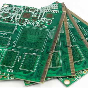
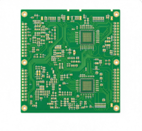
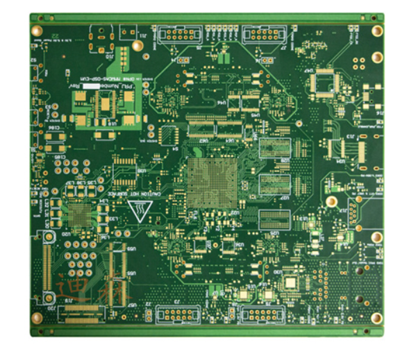
- Board Type: High Density Interconnect (HDI) PCB
- Via Structure: Blind vias (outer layer to inner layer) and Buried vias (inner layer to inner layer)
- Micro-Via Diameter: 0.1mm – 0.2mm (laser drilled)
- Mechanical Via Diameter: 0.2mm – 0.3mm (PTH)
- Layer Count: 4L / 6L / 8L / 10L / 12L, custom stackup available
- Base Material: FR-4 / High Tg FR-4 / High-frequency low Dk/Df material optional
- Board Thickness: 0.4mm – 2.4mm, customizable
- Copper Weight: 0.5oz (18μm) / 1oz (35μm) / 2oz (70μm)
- Minimum Trace / Space: 0.075mm / 0.075mm (outer), 0.1mm / 0.1mm (inner)
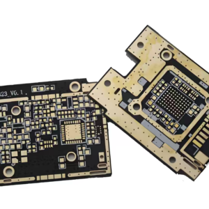
- Solder Mask: Green / Black / Blue / Red / White LPI, UL94 V-0
- Surface Finish: ENIG (Immersion Gold) / OSP / HASL-LF / Immersion Silver
- Impedance Control: Single-ended ±10%, Differential ±10%
- Aspect Ratio: Up to 8:1 for mechanical vias
- Registration Accuracy: ±25μm (layer-to-layer alignment)
- Certification: UL, RoHS 2.0, REACH, IPC-6012 Class 2/3
- Electrical Test: 100% flying probe / fixture test + AOI + X-ray inspection
2. Performance Characteristics
- High interconnection density: blind and buried micro-vias eliminate long through-hole traces, enabling finer routing and higher board wiring capacity
- Reduced board size and weight: HDI technology allows more components on smaller board area compared to traditional through-hole PCB
- Better signal integrity: shorter via stubs reduce signal reflection and parasitic capacitance, improving high-speed signal transmission performance
- Controlled impedance: stackup design optimized for controlled impedance lines, ensuring stable signal quality for high-speed digital circuits
- Improved electrical performance: reduced crosstalk between adjacent traces due to finer pitch and dedicated ground planes
- High reliability: buried vias are sealed inside the board, reducing risk of solder wicking and short circuits during assembly
- Better thermal performance: optimized stackup with dedicated ground and power planes improves heat dissipation across the board
- Higher component placement density: supports BGA, QFP and fine-pitch IC packages with via-in-pad design (optional)
3. Solder Mask Properties
- LPI (Liquid Photoimageable) solder mask applied on outer layers
- Standard green mask; black, blue, red and white colors available on request
- Mask thickness: 10–25μm, consistent across the board
- Strong adhesion to copper surface, resistant to reflow soldering heat
- Good insulation resistance, prevents short circuits between fine-pitch traces
- UV-resistant and weather-stable, suitable for long-term outdoor and industrial use
- White silkscreen legend provides clear component placement identification
- Black mask option available for optical and camera applications requiring low light reflection
- No solder mask bridging on fine-pitch pads, ensures clean soldering during SMT assembly
4. Manufacturing & Process Advantages
- Custom stackup design: our engineering team works with customers to optimize layer stacking based on signal, power and impedance requirements
- Laser drilling capability for micro-vias: precise control of via diameter and depth, supports both blind and buried via structures
- Sequential lamination process: builds up layer by layer to accommodate buried and blind vias with high alignment accuracy
- X-ray inspection: 100% X-ray scan of inner layer registration and via quality before final lamination
- Via-in-pad (VIP) technology available: saves board space by placing vias directly under BGA pads, filled and capped for flat SMT surface
- DFM review provided: flags potential design for manufacturing issues before production starts
- Supports both prototype and volume orders with consistent quality
- Panel optimization: maximizes number of boards per panel to reduce cost for mass production
- Strict layer-to-layer registration control ensures reliable interconnection across all HDI layers
5. Typical Applications
- Mobile phones, tablets and wearable devices requiring compact board size
- BGA and fine-pitch IC packages, high-speed digital processing boards
- 5G communication modules, baseband processing units and antenna modules
- Medical devices: portable diagnostic equipment, patient monitoring systems
- Automotive electronics: ADAS control units, infotainment systems, sensor modules
- Industrial control: PLC boards, motor control units, industrial IoT gateways
- Aerospace and defense (non-classified): avionics control modules, onboard computing units
- High-speed networking: router and switch boards, server interface cards, optical transceiver modules
- Camera and imaging equipment, test and measurement instruments
6. About Us
We are a professional PCB manufacturer based in China, specializing in OEM/ODM custom printed circuit board production for global customers. With years of manufacturing experience, we provide one-stop PCB solutions covering standard FR-4 boards, aluminum MCPCBs, HDI boards, high-frequency boards, ceramic substrates and rigid-flex PCBs.
Our factory is equipped with advanced production lines and testing facilities, ensuring reliable quality from prototype to mass production. We strictly follow IPC standards and hold UL, RoHS and REACH certifications. Our engineering team provides DFM feedback, technical support and fast response to customer inquiries.
We serve customers across Europe, North America, Russia, Southeast Asia and other regions, delivering stable quality, competitive pricing and on-time delivery. Whether you need a small batch prototype or high-volume production, we are ready to support your project.