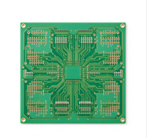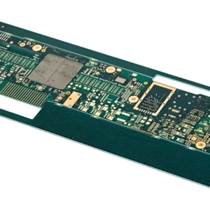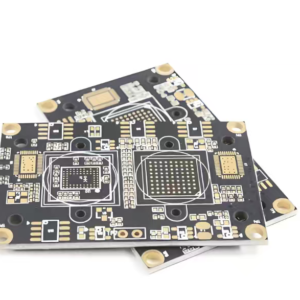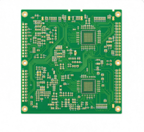
Our Custom 2+N+2 HDI Board, 0.1mm Laser Via, 4-16L Stackup is a sequential laminated HDI circuit board designed for high density BGA fanout and high-speed signal transmission.
Product Overview
Our Custom 2+N+2 HDI Board adopts classic Any-layer style 2+N+2 sequential lamination stack-up structure. The outer two layers are HDI microvia layers connected by 0.1mm laser blind vias, while the inner N layers form the core multilayer routing area.
This structure solves high-density BGA fan-out wiring bottlenecks. Ultra-small laser vias realize pad-on-via, stacked vias layout, greatly save routing space. It is widely customized for high-speed, miniaturized electronic products requiring compact BGA packaging. We support prototype quick turn and mass production, with strict impedance and warpage control.
Core Advantages
✅ Classic 2+N+2 HDI stack-up, mature sequential lamination process, stable yield
✅ Ultra-small 0.1mm laser microvia, support stacked vias & pad-on-via design for dense BGA fanout
✅ 4~16 layers flexible stackup options, match different high-speed routing requirements
✅ Fine trace capability, achieve high-density interconnection in limited board space
✅ Precise differential impedance control, low crosstalk, excellent high-speed signal integrity
✅ Symmetric stack design, effectively reduce board warpage during SMT reflow
✅ Compatible with high-Tg, low Dk/Df material options for high-speed signal
✅ IPC Class2 / Class3 reliability available, RoHS & REACH compliant
Technical Specification Table
| Item | Specification |
|---|---|
| Stack Structure | 2+N+2 HDI, sequential lamination |
| Total Layers | 4L ~ 16L customizable |
| Laser Microvia | Min 0.1mm laser blind via, stacked via allowed |
| Min Line / Space | 3mil / 3mil |
| Base Material | FR4 High-Tg, low loss high-speed FR4 optional |
| Copper Foil | 0.33oz / 0.5oz / 1oz |
| Impedance Tolerance | ±5%, ±8% optional |
| Surface Finish | Immersion Gold, OSP, Immersion Silver, Hard Gold |
| Solder Mask | LPI green / black / blue / red / yellow |
| Board Thickness | 0.6mm ~ 2.0mm |
| Operating Temp | -40℃ ~ 130℃, High-Tg version up to 170℃ |
| Standard | IPC-6012, RoHS, REACH |
Performance & Process Advantages
- Stacked microvia capability: 0.1mm laser via enables pad-on-via layout, maximize routing channels under BGA packages
- Stable sequential lamination: Separate pressing step by step, good interlayer alignment accuracy for multi-layer HDI
- Controlled signal integrity: Low skew routing, suitable for DDR, PCIe, USB high-speed differential signals
- Low warpage performance: Balanced copper distribution + symmetric 2+N+2 stack, ensure stable SMT pick-and-place
- High reliability: Laser via wall quality inspection by X-ray, avoid void and delamination risk
- Full inspection workflow: LDI exposure, AOI, X-ray inner layer check, 100% electrical continuity test
Typical Application Scenarios
- High-speed computing module, SOC mainboard with BGA chip
- 5G communication miniature control board
- High-end camera & image processing module
- Portable industrial test equipment
- Automotive high-density ECU electronic board
- Medical mini precision electronic device