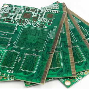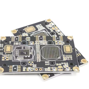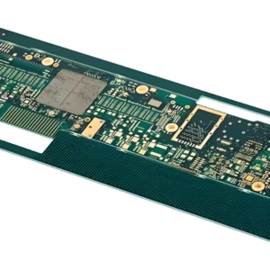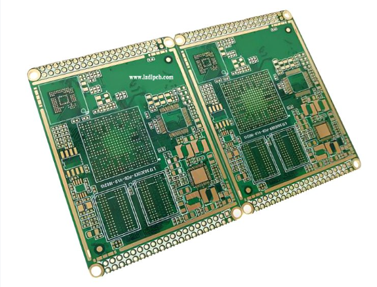
12-Layer HDI Board 6-Step Any-Layer PCB for 5G Processing is a high-density high-speed circuit board designed for 5G signal processing systems.
1. Specifications
– PCB Type: 12-Layer HDI PCB, 6-Step Any-Layer Interconnection
– Stackup: Any-layer sequential lamination, 6-stage laser microvia process
– Base Material: FR-4 / High TG FR-4 / High-frequency low Dk/Df material (Isola, Rogers optional)
– Board Thickness: 0.8mm ~ 2.0mm (customized)
– Minimum Laser Microvia: 0.075mm via hole; 0.12mm pad
– Trace Width / Space: Min 0.05mm / 0.05mm
– Copper Weight: 0.5oz ~ 2oz (inner / outer layer customizable)
– Solder Mask: LPI green/black/blue/red, UL94 V-0
– Surface Finish: ENIG (Immersion Gold), Immersion Silver, OSP, Hard Gold Plating
– Impedance Control: ±5%, ±10% controlled differential & single-ended impedance
– Hole Tolerance: ±0.05mm
– Panel Size: Max 520×620mm
– Minimum Routing Keep-out: 0.08mm
– Certification: IPC-6012 Class 3, UL, RoHS 2.0, REACH
2. Signal & Electrical Performance
– Controlled differential impedance design for high-speed 5G baseband & RF signal transmission
– Low insertion loss, low crosstalk, stable signal integrity at high-frequency bandwidth
– Low Dk / Low Df dielectric option available to reduce high-frequency signal attenuation
– Excellent impedance consistency across the whole panel for high-speed serial links
– Good insulation resistance and dielectric breakdown strength
– Low skew differential pair routing, minimizes timing error for high-speed digital chips
– Stable electrical performance under continuous high-temperature operation for 5G processor modules
– Low leakage current; suitable for high-density power distribution network (PDN)
3. Manufacturing & Process Advantages
– 6-step any-layer HDI structure: interlayer conduction between any layers, not limited by regular sequential HDI
– Stacked & staggered laser microvias supported, ultra-high layer interconnection density
– Greatly saves board space, supports compact miniaturized 5G processor modules
– Fine line & fine space capability to route massive high-speed differential signals
– Precise lamination & layer registration, high alignment accuracy for multi-stage lamination
– Strict impedance testing via TDR, guarantee mass-production consistency
– Support buried resistance / buried capacitance built-in structure (optional)
– Higher reliability than blind-buried via HDI; fewer via stubs to eliminate signal reflection
– Meet IPC Class 3 high-reliability requirement for long-lifecycle communication equipment
4. Typical Applications
– 5G baseband processing boards, 5G macro & small cell communication modules
– High-speed network processor, FPGA core board for communication infrastructure
– 5G industrial gateway, edge computing & industrial communication equipment
– High-performance server communication interface card
– RF & high-speed mixed-signal integrated modules
– Advanced optical communication transceiver boards
– Aerospace & high-reliability data transmission hardware (non-military)