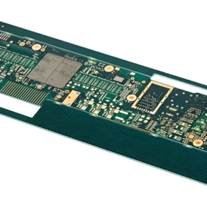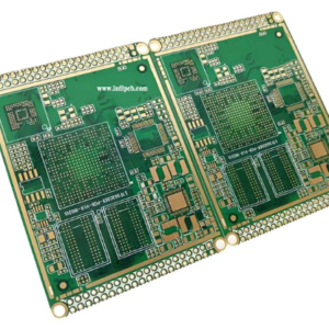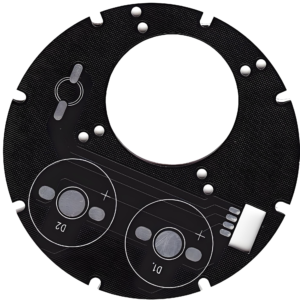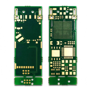
High Density Interconnect PCB (HDI PCB) features fine lines, microvias and high wiring density, saving board space and improving signal integrity. It is widely applied in consumer electronics, medical devices, wearable gadgets and communication modules.
Parameter specification
- Line width/spacing: Standard 4/4–3/3 mil, fine 2.5/2.5 mil, high-end 1.5/1.5 mil (high-end requires specialized processes and equipment).
- Microhole: laser hole diameter 0.075~0.15mm (commonly used is 0.1mm), disk diameter ≤0.25~0.4mm.
- Depth-to-diameter ratio: generally ≤1:1 for microvias (to ensure reliable copper-filling plating); ≤8–10:1 for mechanical through-holes.
- Dielectric: The laminated dielectric layer is very thin (ranging from a few to several tens of micrometers), which is key to miniaturization.
- Microvia filling: Blind vias require copper filling via electroplating (to ensure the reliability of stacked vias and support stacked pads) or resin plugging.
Performance characteristics
- High-density miniaturization: The number of traces and vias per unit area is exponentially increased, enabling thinner and lighter products.
- Excellent signal integrity: Micro-via interconnects offer short signal paths and low parasitic capacitance/inductance, resulting in reduced high-speed signal loss and greater timing stability—ideal for GHz-range high-frequency applications.
- Heat dissipation: Large copper ground or power planes can be arranged in the inner layers to assist with heat conduction.
- Reliability: Copper-filled microvias support “via-on-pad” configurations, enhancing interconnect reliability; however, interlayer alignment and voids within the filled vias are critical failure points.
Design principle
- Sequential Build-up: Laser drilling, copper plating, and lamination are performed layer by layer according to the sequence, enabling interconnection between any internal layers.
- Via configuration: laser microvias for outer layers, mechanical/buried vias for the core, and through-holes spanning all layers—balancing density, cost, and manufacturability.
- Impedance control: achieved through precise design of dielectric thickness, trace width, and reference plane spacing, as well as equal trace lengths for differential pairs and impedance matching.
- Stacked vs. Staggered Vias: Stacked vias offer high density but demand high reliability (requiring copper filling); staggered vias offer greater process latitude and lower costs.
- Prioritize DFM: Costs double with each increase in layer count, so opt for lower layer counts whenever possible; verify microvia pad diameters, edge-to-via spacing, and via-filling capabilities against process limits.
Applicable scenarios
- Consumer electronics: smartphones, wearables, laptops, digital cameras.
- Telecommunications / Servers: 5G base stations, switches, AI accelerator cards (typically featuring any-layer interconnects + high-speed materials).
- Medical: Ultrasound, patient monitors, wearable medical devices.
- Automotive Electronics: ADAS, in-vehicle infotainment systems, and ECU miniaturized modules.
- Industrial Control / IoT: Sensor modules, miniature power modules.
Volectronics Tech Co., Ltd , as a professional PCB manufacturer, we have a strong engineering team, who can check gerber file sent from customers carefully and raise some useful suggestions.
Welcome to contact us for a quote!