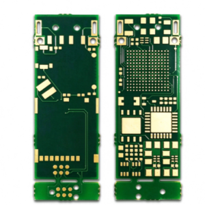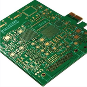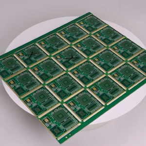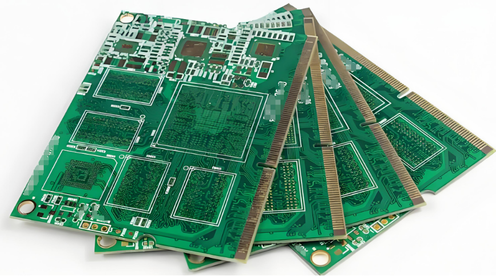
High TG HDI Multilayer PCB features high-density interconnection design with high TG material, ideal for compact electronics, medical devices and automotive electronics. We support custom layer count, blind & buried vias, strict impedance control and quick prototype service.
Key specifications
| Item | Typical Value |
|---|---|
| Layers | 6–20 layers |
| HDI Level | 1st/2nd/3rd order, Any-layer |
| Material | High Tg FR4 (170°C+), Low-Df optional |
| Microvia | 0.075–0.15 mm laser, aspect ratio ≤1:1 |
| Via Type | Blind / Buried / Through hole |
| Min Trace/Space | 3/3–2/2 mil |
| Min Hole Size | 0.1 mm (laser); 0.2 mm (mechanical) |
| Copper Thickness | 1 oz (thin, for fine pitch) |
| Board Thickness | 0.4–2.4 mm |
| Impedance Control | 50/100Ω, ±10% |
| Via Filling | Copper plug / resin plug |
| Surface Finish | ENIG / Immersion Tin / OSP |
| Solder Mask | Green/Black LPI |
Manufacturing Features
- Micro-via technology: Laser-drilled micro-vias (0.075–0.15 mm) formed via sequential build-up; aspect ratio ≤1:1.
- Blind/Buried vias: Connect only specific layers, freeing up routing space.
- Copper-filled plating: Copper-filled micro-vias supporting via-in-pad designs, enhancing density and reliability.
- Sequential build-up: Layer-by-layer lamination, laser drilling, and plating to achieve Any-Layer Interconnect (ALIC).
- High-Tg materials: Resistant to thermal stress from multiple reflow cycles and thermal deformation.
- Stacked vs. Staggered vias: Stacked vias offer high density (require copper filling); staggered vias offer process tolerance and lower cost.
Signal Performance
- Short signal paths: Micro-via interconnects minimize path length, reducing parasitic capacitance and inductance while lowering high-speed signal loss.
- Controlled impedance: Precision control (e.g., 50Ω/100Ω) and matched differential pair lengths.
- Low-loss materials: Options for low-Df materials to enhance high-speed signal integrity.
- Continuous power/ground planes: Low noise and robust EMI suppression.
- Suitable for high-speed applications: Telecommunications, servers, AI, and high-speed digital interconnects.
Volectronics Tech Co., Ltd is a one-stop service provider for PCB and PCBA manufacturing, covering the entire production chain under one roof — from PCB design and fabrication to component sourcing, assembly, and functional testing.
If you require additional process like Dielectric Thickness, Impendance Control, Mask Tented, Counter Sink, Counter Bore, Blind/Buried Vias, Carbon Ink, Edge Plating, Via in Pad and Silver Filled Vias.
Welocme to feel free to contact us!