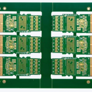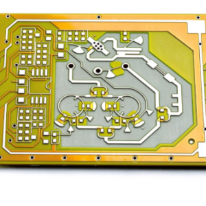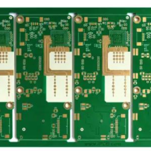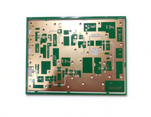
High-Speed Digital & High Frequency RF Microwave PCB covers 6 to 40 layers, supporting hybrid stack-up of high-frequency microwave materials and low-loss high-speed substrates for mixed-signal circuits. It is widely used for 6~40GHz microwave transmission, millimeter wave radar, 5G/6G radio and high-speed SerDes interconnection, with strictly controlled impedance and ultra-low signal loss.
Specifications
- Layer Count: 6 ~ 40 layers, hybrid stack-up (high-frequency laminate + high-speed FR4 / Megtron / Isola) available
- Base Materials: Rogers RO4003C / RO4350B / RT5880, Taconic, Isola I-Tera MT, Megtron 6, high Tg low-loss FR4
- Dk Range: 2.2 ~ 3.7 (tight Dk tolerance ±0.05 for RF layers)
- Df (Dissipation Factor): 0.0009 ~ 0.0045, ultra-low loss for microwave bands
- Board Thickness: 0.8mm ~ 6.0mm, customized
- Copper Foil: Low-profile / ultra-low-profile copper 0.5oz ~ 2oz, optimized for skin effect
- Min Line Width / Space: 3mil / 3mil; laser microvia down to 75μm
- Surface Finish: ENIG, Immersion Silver, OSP, Hard Gold, Immersion Tin
- Solder Mask: LPI liquid mask, thin mask option for RF traces; green/black/blue customizable
- Minimum Hole: Mechanical 0.15mm, laser microvia 0.075mm
- Tolerance: Outline ±0.075mm, layer-to-layer alignment ±0.05mm
- Compliance: RoHS, REACH, IPC-6012 Class 2 / Class 3
Manufacturing Advantages
- Hybrid lamination technology: separate RF signal layers and high-speed digital layers, balance RF loss and cost
- Sequential lamination for high layer count up to 40L, stable board warpage control
- Laser drilling & backdrilling service, eliminate via stub parasitic effect critical for microwave
- Low-roughness copper process to reduce conductor loss at 6–40GHz
- Etch compensation & stack-up simulation before production, consistent trace geometry
- TDR & VNA testing for impedance validation, AOI + AXI + flying probe 100% electrical test
- Strict DFM review for mixed-signal isolation, stitching ground vias, cavity design if needed
- Support cavity PCB, castellated edge, buried capacitor/resistor integration
- Prototype & volume run capability, vacuum packing to avoid moisture absorption of high-frequency material
Impedance Characteristics
- Standard RF single-ended: 50Ω (±2% / ±5% tolerance); 75Ω optional
- High-speed differential pair: 85Ω, 100Ω, 120Ω, tolerance ±5%
- Supported transmission structures: Microstrip, Stripline, GCPW grounded coplanar waveguide
- Impedance calculated by stack-up Dk, dielectric thickness, trace width, copper thickness
- Continuous impedance transition at via / connector pad, minimize reflection & VSWR
- TDR impedance test coupon included for verification; full VNA S-parameter test available for high-end requirement
- Stable impedance over wide temperature range (-55℃ ~ +125℃), low phase drift for phased array
Signal Performance
- Operating frequency coverage: DC up to 40GHz, support microwave, Ka-band, high-speed SerDes
- Low insertion loss & low return loss; typical VSWR ≤1.5 for RF channels
- Optimized ground plane design, suppress crosstalk between digital high-speed lanes and RF microwave traces
- Low jitter for high-speed digital signals (PCIe, DDR, SerDes), good eye diagram performance
- Reduce skin-effect and dielectric loss with low Df laminate and smooth copper
- Isolation improvement by ground stitching vias and shielded layout, avoid digital noise coupling into RF front-end
- Consistent propagation delay, suitable for phase-sensitive radar and beamforming systems
Application Scenarios
- 5G / 6G communication, microwave backhaul, Ka-band radio unit
- Automotive millimeter-wave radar, ADAS sensor modules
- Phased array antenna, satellite communication, aerospace RF transceiver
- High-speed test & measurement instruments, signal generators, spectrum analyzers
- High-speed computing, server high-speed interconnect, optical transceiver boards
- Industrial microwave sensing, security radar, wireless RF front-end modules
About Our Company
We provide full DFM simulation, stack-up design, prototype validation and mass production service for complex high-frequency high-speed PCBs. Our test lab supports TDR, VNA impedance & S-parameter measurement. Flexible delivery and technical support for RF and high-speed mixed-signal projects.