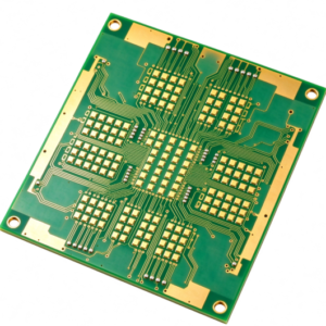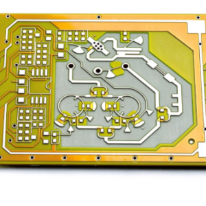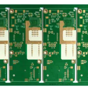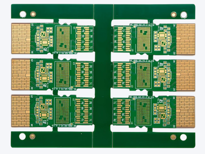
Our 8-12L High-Frequency PCB adopts low-loss dielectric substrate, specially designed for AI high-speed interconnection and 5G RF front-end applications.
Core Selling Points
🟢 8–12 stack layers, low-loss dielectric substrate, excellent signal integrity for high-speed & RF signals
🟢 Hybrid stackup support: Rogers / PTFE + FR4, balance high-frequency performance and cost
🟢 Tight impedance control ±5% / ±8%, stable Dk & ultra-low Df under wide frequency band
🟢 Designed for AI accelerator board, 5G RU, millimeter-wave communication and high-speed computing modules
🟢 Fine line & microvia technology, suitable for dense BGA, high pin count chips routing
🟢 Strict IPC Class 2 / Class3 available, 100% electrical test before delivery
🟢 OEM & prototype service, DFM review at early stage to reduce design risk
🟢 RoHS & REACH compliant, long-term stable performance under continuous high-load operation
Specification Table
| Item | Specification |
|---|---|
| Layer Count | 8L / 10L / 12L customizable |
| Base Material | Rogers (RO4003C, RO4350B, RO5880), PTFE, ceramic filled RF material, hybrid Rogers+FR4 |
| Dielectric Constant Dk | 2.2 ~ 10.2 (depends on material) |
| Dissipation Factor Df | 0.0009 ~ 0.003 @10GHz |
| Copper Foil | Low profile copper / RTF reverse treated foil / ED copper |
| Impedance Control | Single-ended / differential impedance, tolerance ±5%, ±8%, ±10% |
| Min Line / Space | 3mil / 3mil |
| Microvia | Laser blind & buried microvia available |
| Board Thickness | 0.8mm ~ 3.2mm custom |
| Surface Finish | Immersion Gold, Hard Gold, OSP, Immersion Silver, Immersion Tin |
| Solder Mask | LPI solder mask; bare copper optional for RF antenna area |
| Working Frequency | Up to mmWave band (24GHz, 28GHz, 39GHz, 77GHz) |
| Application Band | 5G, high-speed SerDes, AI high-speed interconnection |
| Quality Standard | IPC-6012, RoHS, REACH |
Performance Characteristics
- Ultra-low insertion loss: Low-loss substrate greatly reduces RF & high-speed signal attenuation, avoid bit error for AI high-speed serial links
- Stable dielectric property: Dk hardly drifts with temperature, humidity and frequency, consistent phase performance for 5G RF front-end
- Low CTE: Good dimensional stability during multiple reflow cycles, less risk of via crack and delamination
- High isolation between layers: Reasonable stack-up ground plane design, suppress crosstalk between high-speed differential pairs and RF traces
- High heat dissipation compatibility: Can combine thick copper design for AI boards with high power consumption
- Low moisture absorption: Electrical performance won’t drift in humid working environment
Manufacturing & Process Advantages
- Professional multi-layer RF stack-up engineering team, accurate calculation for stripline, microstrip, GCPW structure
- Special lamination process for low-loss RF material, control pressure & temperature precisely to prevent void, delamination and warpage
- Laser drilling for blind/buried microvias, high alignment accuracy for dense multi-layer layout
- Special low-loss etching process, keep copper surface smooth to minimize conductor loss
- TDR impedance testing service available, provide test report on request
- Hybrid stack-up capability: digital layers on FR4, RF high-frequency layers on Rogers, effectively save customer cost
- Multi-step AOI + electrical open/short test for each layer, reduce hidden defect rate of complex 8–12L boards
- Support controlled depth routing, backdrilling for high-speed SerDes signal optimization
Design Principle
8–12 layer high-frequency PCB separates RF signal, high-speed differential signal, power and ground into different layers by scientific stack-up arrangement. Ground reference planes are placed adjacent to RF / high-speed traces to stabilize impedance and suppress interference. For AI & 5G scenarios, many circuits contain both analog RF signal and high-speed digital SerDes signal, hybrid stack-up is widely adopted: use expensive low-loss Rogers/PTFE only for RF layers, use FR4 for power and digital layers. Backdrilling and microvia design are often applied to reduce stub length, which is critical to eliminate signal reflection at high frequency and high speed.
Typical Application Scenarios
- 5G Remote Radio Unit (RU), 5G macro & small cell base station
- AI high-speed accelerator board, high-speed computing interconnection card
- Millimeter wave radar, phased array antenna system
- High-speed network switch, optical communication module
- RF power amplifier, filter, transceiver module
- Test & measurement high-frequency instrument
Company Brief
We are a professional PCB manufacturer focusing on custom high-frequency, HDI, rigid-flex, FPC and metal core MCPCB boards.
With rich experience in complex multi-layer RF circuit fabrication, we serve global customers in 5G, AI, radar, industrial control and medical electronics. We provide one-stop service including DFM review, prototype sampling, small batch and mass production. Strict quality control system and fast communication help customers shorten product development cycle. All products comply with IPC, RoHS and REACH standards.