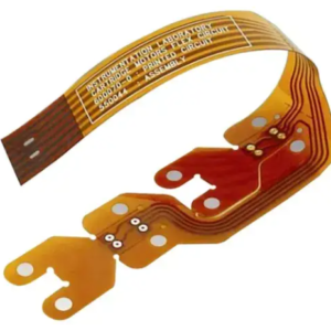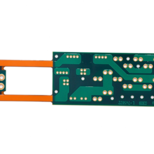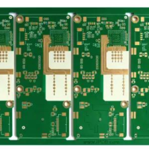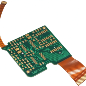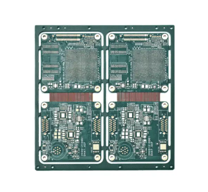
Our Custom Rigid Flex Circuit Board combines rigid FR4 sections and flexible polyimide layers. This Rigid Flex Circuit Board enables folding and 3D assembly for compact electronic devices like medical instruments, wearable electronics and aerospace modules. We offer custom layer stack-up, impedance control and reliable quick-turn PCB prototyping & mass production.
Specifications
| Item | Typical Value |
|---|---|
| Construction | Rigid multilayer + Flex core layers (integrated) |
| Rigid Material | FR4, High Tg (150–170°C) |
| Flex Substrate | Polyimide (PI) 12.5–25μm, RA/ED copper |
| Layers | Rigid 4–12L + Flex layers |
| Min Trace/Space | 4/4–3/3 mil (Flex area) |
| Min Hole Size | 0.2 mm mechanical; microvia for HDI |
| Bend Radius | Dynamic ≥10× thickness; Static ≥3× |
| Flex Life | 10k–100k+ cycles (RA copper) |
| Operating Temp. | −65 ~ +150°C |
| Impedance Control | 50/100Ω controlled |
| Surface Finish | ENIG (Ni/Au) / Immersion Gold |
| Solder Mask / Coverlay | PI coverlay on flex area; LPI on rigid area |
Design Principle
- Rigid zones support components (e.g., BGAs, connectors), while flexible zones accommodate bending, folding, and 3D assembly.
- Position the flexible layer at the center (neutral axis) to minimize the stress differential between the inner and outer layers during bending.
- Route traces in bending zones perpendicular to the bend axis; prohibit vias, pads, or openings (which act as stress concentration points).
- Incorporate extended buffer sections (flexible extensions) at rigid-flex transition zones to prevent tearing and stress concentration.
- Use a symmetrical stack-up to ensure flatness and manufacturability.
- Multi-layer lamination combined with laser via formation; flexible and rigid layers are laminated into a single integrated structure.
- Uses rolled-annealed (RA) copper and polyimide (PI) coverlay for dynamic bending applications to enhance flex life.
- High interlayer alignment precision; controlled resin flow to prevent delamination.
- Rounded corners at coverlay openings in bending zones to prevent stress-induced fractures.
- Reliability validation includes thermal cycling, temperature-humidity testing, flex life testing, and dielectric withstand voltage testing.
- Controlled impedance for microstrip and stripline configurations supports high-speed differential signals.
- Multi-layer internal shielding reduces crosstalk.
- Impedance margins are factored into bend areas, and high-speed signal paths avoid zones with sharp bends.
- Suitable for high-density interconnects and miniaturization requirements in compact devices.
Volectronics Tech Co., Ltd is a one-stop service provider for PCB and PCBA manufacturing, covering the entire production chain under one roof — from PCB design and fabrication to component sourcing, assembly, and functional testing. Whether you need quick-turn prototypes or volume production, we deliver complete, quality-controlled solutions from a single, reliable partner.
Welocme to feel free to contact us!