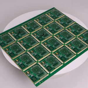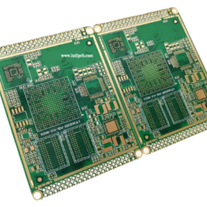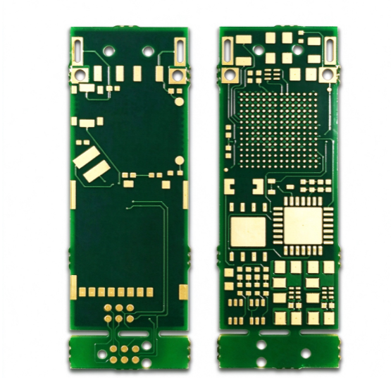
Volectronics manufactures Multilayers HDI PCB with BGA Pad, Immersion Gold Finish, delivering high-density interconnect boards engineered for BGA packages in communication, server, AI, and high-speed digital applications. These boards combine microvia build-up technology with copper-filled via-in-pad, controlled impedance, and ENIG surface finish to support fine-pitch BGAs with reliable solder joints and excellent electrical performance.
Specifications
| Item | Typical Value |
|---|---|
| Layers | 6–20 layers (HDI) |
| HDI Level | 1st/2nd/3rd order, Any-layer |
| Material | High Tg FR4 (170°C+), Low-Df optional |
| Microvia | 0.075–0.15 mm laser, aspect ≤1:1 |
| Via-in-Pad | Copper-filled, supported |
| BGA Pad | Via-in-pad / NSMD / SMD pad types |
| Min Trace/Space | 3/3–2/2 mil |
| Min Hole Size | 0.1 mm (laser); 0.2 mm (mechanical) |
| Impedance Control | 50/100Ω, ±10% |
| Surface Finish | Immersion Gold (ENIG) |
| Solder Mask | Green/Black LPI, via tenting |
| Operating Temp. | −40 ~ +150°C |
| Flatness / Coplanarity | High (BGA assembly) |
| UL Rating | UL 94V-0 |
Design Principle
– Microvia Build-up: Sequential build-up using blind and/or buried vias to achieve high-density interconnection.
– Via-in-pad: Vias placed directly within BGA pads to conserve routing space and increase density.
– Copper-filled Microvias: Copper-filled via-in-pad structures providing a planar surface, suitable for BGA mounting and reflow soldering.
– BGA Pad Design: Optimized NSMD (Non-Solder Mask Defined) or SMD (Solder Mask Defined) pads to ensure reliable component mounting and solder joints.
– Symmetrical Stack-up: Balanced layer configuration with continuous power/ground planes, ensuring stable reference for signals.
Signal & Electrical Performance
– Short signal paths: Micro-via interconnects are short, resulting in low parasitic capacitance/inductance and minimal high-speed signal loss.
– Controlled impedance: Precise 50/100Ω control with matched-length differential pairs.
– Low-loss material options: Enhanced high-speed signal integrity.
– Continuous ground planes: Reduced crosstalk and robust EMI suppression.
– Ideal for high-speed digital applications: Including telecommunications, servers, AI, and high-density BGA packaging.
Manufacturing Advantages
- High-Tg Materials: Resistant to thermal stress from multiple reflow soldering cycles; highly resistant to thermal deformation.
- Copper-Filled Vias (Plated): Supports “via-in-pad” designs; ensures a flat surface and reliable solder joints.
- Electroless Nickel Immersion Gold (ENIG): Provides a flat, coplanar surface with excellent solderability and a long shelf life; ideal for BGA components.
- Microvia Build-up (HDI): Enables high routing density and facilitates BGA fan-out.
- BGA Coplanarity Control: Specialized manufacturing processes ensure pad coplanarity, resulting in high assembly yields.
- Reliability Validation: Includes thermal cycling, temperature-humidity testing, and X-ray inspection of BGA solder joints.
Typical Applications
- Communication base stations and switches
- Servers and data centers
- AI accelerators and high-speed modules
- Networking and high-density BGA assemblies
Volectronics delivers reliable, high-performance Multilayers HDI PCB with BGA Pad solutions for high-density, high-speed electronics. Contact us for a custom quote on your HDI board design.