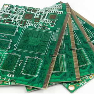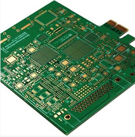
Prototype Custom Fine Pitch BGA HDI PCB with Microvias is a high-density interconnect circuit board built with laser drilled microvias, blind & buried vias and optional via-in-pad, specially engineered for fine-pitch BGA chips on compact high-speed electronics.
I. Key Benefits
✅ Laser microvia, blind & buried via structure, supports fine-pitch BGA layout, greatly improves routing density for compact chips
✅ Via-in-pad available, eliminates escape routing bottleneck under BGA, save board space for miniaturized design
✅ Ultra-fine line & space capability, suitable for high-speed differential signals with tight impedance tolerance
✅ Fast prototype service for engineering verification, short turnaround for R&D projects
✅ Stable dielectric material option for high-speed signal, low loss, low skew for DDR, PCIe, high-speed serial links
✅ Precise layer alignment and impedance control, reduce crosstalk and signal attenuation
✅ Stack-up customized according to your BGA pitch, signal requirement and thermal dissipation demand
✅ IPC-A-600 Class 2 / Class 3 available for industrial, medical and communication high-reliability applications
II. Specifications
| Item | Specification |
|---|---|
| Product Name | Prototype Custom Fine Pitch BGA HDI PCB with Microvias |
| Structure | HDI, 1+n+1 / 2+n+2 stack-up, laser microvias, blind vias, buried vias, via-in-pad |
| Base Material | FR-4, High Tg FR4, Low Dk/Df high-speed material (Isola, Rogers, Shengyi etc.) |
| BGA Pitch Support | 0.4mm / 0.5mm / 0.65mm / 0.8mm fine pitch BGA |
| Min Line / Space | 0.05mm / 0.05mm |
| Min Microvia Diameter | 0.075mm laser microvia |
| Copper Thickness | 0.25oz, 0.5oz, 1oz (inner / outer layer customized) |
| Surface Finish | ENIG, ENEPIG, Hard Gold, OSP, Immersion Silver |
| Impedance Tolerance | ±5% / ±10% customized |
| Layer Count | 4~20 layers |
| Operating Temperature | -40℃ ~ 130℃ (depends on substrate Tg) |
| Tolerance | Outline ±0.10mm, hole position ±0.05mm |
| Reliability Grade | IPC Class 2 / Class 3 |
III. Design Principle
This HDI PCB adopts a high-density interconnect stack-up designed specifically for fine-pitch BGA packages.
- Traditional through-hole cannot escape traces underneath small-pitch BGA balls. Laser microvias directly connect pads to inner signal layers, solving the routing escape problem.
- Via-in-pad technology puts microvias right under BGA solder pads, removing the need for fan-out traces around the pad, which is the core for 0.4/0.5mm ultra-fine pitch BGA.
- The stack-up is arranged with reference planes adjacent to signal layers, to control impedance, shorten return path and suppress EMI.
- High-speed differential pairs are routed with consistent gap and length matching to minimize skew and crosstalk.
- Thermal vias array can be added under large BGA chips to improve heat dissipation and reduce junction temperature.
- Layer sequence, dielectric thickness and copper weight are matched together to meet your impedance specification.
IV. Signal & Electrical Performance Features
- Supports tight impedance control for single-ended and differential pairs: USB, PCIe, DDR, Ethernet and other high-speed interfaces.
- Low Dk/Df high-speed substrate option reduces insertion loss at high frequency, maintains signal integrity.
- Short microvia path provides low inductance, better than traditional mechanical drilled holes, good for high-speed chip interfaces.
- Complete ground/power reference plane minimizes return path discontinuity and reduces crosstalk between adjacent traces.
- Controlled trace length matching ensures timing requirement for memory and parallel bus signals.
- DFM review before production: check BGA fan-out risk, impedance risk, voltage drop and thermal bottleneck for your layout.
V. Manufacturing & Process Advantages
- UV laser drilling for microvias: high precision, small hole size, suitable for dense BGA area.
- Sequential lamination process for blind and buried vias, accurate layer registration, less layer shift.
- Special desmear process for laser microvias to guarantee reliable copper plating inside tiny vias, prevent open circuit.
- Advanced AOI + AXI inspection, especially for hidden microvia and via-in-pad quality checking.
- Strict impedance testing with TDR upon request for high-speed boards.
- Mature prototype workflow, fast sampling for engineering test, support design revision iteration.
- Stable registration control, avoid BGA pad shift issue which causes soldering short or open.
VI. Application Scenarios
- High-speed industrial control mainboard
- Image processing & video capture board
- Communication RF and signal processing modules
- Portable high-performance detection equipment
- Medical imaging control PCB
- AI edge computing mini carrier board
- High-density FPGA & SoC carrier board