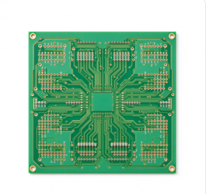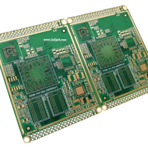
HDI Multilayer PCB is a high-density interconnect circuit board built with FR4 material, equipped with laser BGA microvias and resin plug holes for compact CMOS camera sensor modules.
Custom HDI Multilayer FR4 PCB with BGA microvias and resin plug holes, built for compact high-density electronic modules. It adopts laser microvia technology to fan out fine-pitch BGA chips, greatly reduce board size and improve signal integrity. Widely used in camera modules, industrial control, IoT and communication hardware.
1. Specification & Parameters
- Base Material: FR4, optional High TG FR4
- Layer Count: 4~8 layers (common 4 layers for this IMX323 camera board)
- Min Microvia: 0.1mm laser blind via
- Min trace / space: 0.075mm / 0.075mm
- BGA Pitch: 0.8mm fine pitch
- Surface Finish: ENIG (Electroless Nickel Immersion Gold)
- Solder Mask: Black solder mask (matte black available)
- Process: Laser blind microvia + resin plug hole
- Operating Temp: -40℃ ~ +130℃
- Compliance: IPC-6012 Class 2
2. Manufacturing & Process Advantages
- Laser drilling microvias for BGA fanout, solves routing difficulty for fine pitch BGA.
- Resin plug hole technology: fill blind vias with epoxy resin, flat surface for BGA soldering, prevent air bubble issue during SMT.
- High lamination alignment accuracy, layer offset ≤ ±0.05mm.
- AOI + X-ray inspection for microvia quality check, ensure no void or open circuit inside blind holes.
- Prototype & mass production available, DFM review before fabrication.
- Matte black solder mask option for camera module, reduce light reflection.
3. Signal & Electrical Performance
- Short interconnection path via microvias, lower inductance and insertion loss.
- Good impedance control available for high-speed signals.
- High insulation resistance ≥10¹²Ω, stable dielectric property.
- Low crosstalk for densely routed traces.
- Reliable electrical continuity after thermal cycling test.
4. Design Principle
- Microvias directly under BGA pads to shorten signal path, save routing space.
- Resin filled blind vias to create flat surface for BGA component mounting.
- Stack-up optimized for impedance and noise suppression, critical for image sensor signal.
- Ground plane design to reduce EMI interference for camera module.
5. Application Scenarios
CMOS camera modules (IMX323), IoT modules, small industrial sensors, portable communication electronics.
6. Our Service
We provide custom HDI PCB service including DFM analysis, prototype and mass production. Strict IPC quality control with AOI, X-ray and full electrical test. Flexible lead time for small batch and volume orders.