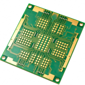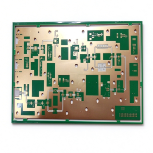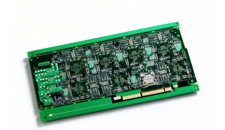
I. Specifications
| Item | Specification |
|---|---|
| Product Name | High Frequency PCB with Edge Connector & Green Guard Band |
| High Frequency Material | Rogers RO4350B / RO4003C / RT5880 / Taconic / Isola / Arlon, hybrid FR4+HF material optional |
| Dk (Dielectric Constant) | 2.2 ~ 10.2 (depends on selected HF substrate) |
| DF (Dissipation Factor) | 0.0009 ~ 0.003 @10GHz |
| Layer Count | 2L / 4L / 6L / 8L, custom stack-up |
| Copper Foil | 1oz (35μm), 0.5oz(18μm), reverse treated foil / low profile copper for low insertion loss |
| Edge Connector (Gold Finger) | Hard gold plating, gold thickness 0.3μm~1.27μm, nickel underlayer 2~5μm |
| Guard Band | Green LPI solder mask guard band, reserved isolation zone between edge connector and RF traces |
| Min Trace / Space | 0.1mm / 0.1mm |
| Impedance Tolerance | ±5%, ±3% (tight tolerance for RF requirement) |
| Operating Frequency | DC ~ 40GHz (material dependent) |
| Operating Temperature | -40℃ ~ +125℃ |
| Surface Finish | ENIG, Hard Gold (Gold Finger), Immersion Silver |
| Board Thickness | 0.508mm, 0.762mm, 1.524mm, custom thickness |
| Outline Tolerance | ±0.075mm |
| Compliance | IPC-6012, RoHS, REACH |
| Special Feature | Precisely defined green solder mask guard band between edge connector area and RF circuit |
II. Performance Features
- Low Dk & low DF high-frequency substrate, ultra-low signal insertion loss at microwave / RF frequency band, stable dielectric constant under frequency change.
- Edge connector (gold finger) design for direct plug-in connection with RF test sockets, backplane and radio frequency modules, no extra connector needed.
- Custom green solder mask guard band separates gold finger contact region and RF signal traces; reduce capacitive coupling, crosstalk and accidental short circuit during plugging.
- Low-profile copper foil minimizes skin effect loss, excellent signal integrity for high-speed differential and single-ended RF transmission lines.
- Support controlled impedance design for microstrip line, coplanar waveguide (CPW), grounded coplanar waveguide (GCPW).
- Hard gold plating on edge connector ensures low & stable contact resistance, thousands of plug/unplug cycles.
- Suitable for RF power amplifier, antenna feed board, radar sensor, 5G/6G communication, RF test fixture, microwave transceiver module.
III. Design Principle
- High frequency stack-up & transmission line design Select low-loss HF laminate. The circuit is designed as microstrip / GCPW transmission line. Dk, substrate thickness and trace width are calculated to reach target impedance (commonly 50Ω for RF). Ground plane provides reference return path and suppress radiation.
- Edge Connector (Gold Finger) principle The edge connector is placed on the board border. Traces extend directly to the board edge as contact fingers. Hard gold plating guarantees stable contact for repeated plugging with mating socket.
- Green Guard Band core design The green guard band is a reserved isolation zone covered by green solder mask, placed between gold fingers and RF signal traces.
- Isolate the exposed gold finger contact area from adjacent RF traces
- Reduce parasitic capacitance coupling between connector and RF circuit
- Prevent solder bridge, scratch short and ESD risk during assembly & testing
- Visible green boundary helps operators distinguish contact area and circuit area visually
Important: Guard band area is non-circuit zone, no copper trace inside the green guard band.
- Impedance continuity Engineers must maintain consistent impedance through the transition from RF trace → guard band zone → gold finger, avoid impedance discontinuity that causes signal reflection and VSWR rise.
IV. Core Manufacturing Advantages
- Professional high-frequency lamination process, control internal stress, avoid substrate delamination and Dk shift after pressing.
- Precision laser drilling / mechanical drilling for HF board, clean hole wall, low signal leakage.
- Accurate exposure & etching for fine RF traces, consistent line width to guarantee impedance stability.
- Precise routing for edge connector: smooth edge cutting, no burr, prevent scratching gold plating and cause contact failure.
- Strict guard mask alignment: the green guard band border is positioned accurately as required, mask offset controlled within ±0.05mm.
- Selective hard gold plating process: only plate gold on edge connector fingers, save cost while meet plugging life requirement.
- 100% AOI + open/short test; sampling impedance & VSWR test available for high-frequency orders.
- Support prototype quick turn and mass production for RF customers.
V. About Our Company
We are an experienced high-frequency PCB manufacturer specializing in low-loss RF circuit boards, edge connector boards, impedance-controlled boards and microwave communication substrates. With a modern production facility in Shenzhen, China, we provide one-stop support from material selection, stack-up design and prototype fabrication to mass production.
Our engineering team understands high-frequency signal integrity, transmission line performance and the special requirements of Rogers, Taconic, Isola and other high-frequency laminates. We work closely with customers in radar, 5G communication, wireless modules, RF test fixtures and industrial electronics to deliver stable, high-quality PCBs with tight impedance tolerance and reliable electrical performance.
Quality control, on-time delivery and responsive technical support are the core of our service. We welcome RF engineers, procurement teams and OEM partners to discuss custom high-frequency PCB projects.