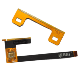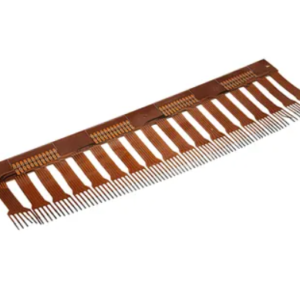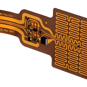
Our Flexible PCB is custom-made Polyimide FPC designed for MDC825 CMOS Camera Module. This fine-trace flexible printed circuit board features high bend resistance and stable high-speed signal transmission for compact imaging devices.
This PI flexible circuit board is customized for MDC825 CMOS camera module, featuring fine traces, high bendability and stable high-speed signal transmission. It connects CMOS image sensor and connector, widely used in miniature camera imaging systems.
1. Specification Parameters
- Base Material: Polyimide (PI), typical thickness 12.5μm / 25μm
- Copper Foil: Rolled annealed copper, 9μm / 12μm
- Layer Count: 2-layer FPC
- Min Line Width / Line Space: 0.05mm / 0.05mm
- Min Hole Diameter: 0.1mm micro via optional
- Surface Finish: Immersion Gold / ENIG (for sensor bonding pad)
- Coverlay: PI coverlay with adhesive, 12.5μm
- Operating Temperature: -40℃ ~ +125℃
- Board Thickness: 0.08mm ~ 0.15mm (customizable)
- Impedance Control: Optional single-ended / differential impedance for high-speed signal
- Bend Cycles: ≥100,000 times under proper bending radius
2. Manufacturing & Process Advantages
- Fine-line fabrication capability to match compact MDC825 CMOS layout, high precision pad array for sensor soldering.
- PI substrate with excellent heat resistance, no deformation during SMT reflow soldering for camera module assembly.
- Stable ENIG gold surface finish, good bonding performance, anti-oxidation for long-term storage.
- Contour routing & laser cutting for complex irregular shape, match camera internal limited space.
- Strict impedance tolerance control for high-speed image signal transmission.
- Low outgassing material, suitable for optical imaging module environment.
- Flexible structure, supports repeated dynamic bending in tiny camera assembly.
3. Signal Performance Characteristics
- Low dielectric loss of PI material, maintains signal integrity for high-speed image data transmission from CMOS sensor.
- Low crosstalk between adjacent fine traces, reduces noise interference to imaging signal.
- Consistent trace geometry, minimal signal attenuation.
- Stable electrical performance under vibration and bending, no intermittent signal dropout.
- Good EMC performance, suppress electromagnetic interference that may cause image noise.
4. Impedance Characteristics
- Support customized single-ended impedance: 50Ω ±10%
- Support differential impedance: 90Ω / 100Ω ±10% (common for camera MIPI signal)
- Impedance controlled by adjusting copper thickness, trace width, coverlay thickness.
- Impedance simulation before production to match MDC825 CMOS MIPI interface requirement.
- Impedance testing on coupon to guarantee consistency in mass production.
5. Application Scenarios
MDC825 CMOS camera module, embedded vision, industrial miniature camera, medical endoscope camera, laptop/tablet camera, automotive auxiliary camera.
Our Services at Volectronics Tech Co., Ltd
We provide one-stop custom Flexible PCB manufacturing service from schematic review, stack-up design, DFM checking, prototype fabrication to mass production.
– Free DFM review before production
– Prototype & volume order support
– Multiple surface finish options: ENIG, Immersion Silver, OSP, HASL
– Impedance control & stack-up customization
– Strict IPC-A-600 quality inspection
– Fast lead time for PCB prototypes
– Professional technical support throughout your project
We can also support subsequent SMT assembly and PCBA service upon request.Welcome to contact us for more details.