
PCB Design for Manufacturing is not optional —— it’s what separates a smooth run from a scrapped batch.You have finished your schematic, laid out your board, and checked your routing. Now the real question: will your PCB actually manufacture cleanly?
DFM — Design for Manufacturing — is the set of design rules that determines whether your board is easy to build, or whether it costs you rework, delays, and scrap. A design that ignores DFM can look perfect on screen and still fail on the line. This guide walks through the seven DFM rules that matter most for a reliable, low-cost PCB.
What Is DFM and Why Does It Matter?
Design for Manufacturing means designing your board with the factory’s capabilities in mind. Every PCB manufacturer has physical limits — minimum trace width, minimum hole size, minimum spacing, and so on. When your design respects those limits, production runs smoothly and yield stays high. When it ignores them, you pay in rework, longer lead times, and scrapped boards.
Understanding DFM is especially important before you send Gerber files to a manufacturer, because most DFM problems are far cheaper to fix in the design stage than on the production line.
DFM Rule 1: Trace Width and Spacing
The width of your copper traces and the space between them must fall within what your manufacturer can reliably etch.
- Minimum trace width— the narrowest trace the factory can produce without defects
- Minimum spacing— the gap between adjacent traces needed to avoid shorts
Wider traces and generous spacing also carry more current and are easier to manufacture, which is why standard production prefers them whenever the design allows.
DFM Rule 2: Pad Size and Land Pattern
Every component needs a pad that matches its package. The pad (or land pattern) must be sized correctly for the component footprint:
- Too small → weak solder joints and poor connections
- Too large → solder bridges and misalignment during placement
Using the manufacturer’s recommended land patterns for each package helps ensure clean, reliable soldering for SMT and through-hole parts alike.
DFM Rule 3: Drill Holes and Vias
Holes and vias connect different layers and mount through-hole components. Your design must respect the factory’s minimum hole size and choose the right via type:
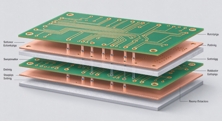
- Through-hole vias— pass through the entire board
- Blind vias— connect an outer layer to an inner layer
- Buried vias— connect inner layers only
Smaller holes and complex via types cost more and add process steps, so it pays to keep hole sizes and via structures as simple as the design allows.
DFM Rule 4: Copper Thickness and Clearance
The thickness of your copper (commonly 1 oz or 2 oz) affects current capacity and impedance. Equally important is clearance — the distance between copper and the board edge or between different nets.
Insufficient clearance risks shorts and manufacturing defects. Leave enough margin between copper and the board outline, and around holes and slots, so the factory can process the board without errors.
DFM Rule 5: Solder Mask and Silkscreen
Two protective layers often get overlooked in the design phase:
- Solder mask— the coating that prevents solder bridges. Openings (windows) must align exactly with the pads, and the mask must not cover areas that need soldering.
- Silkscreen— the printed labels and reference designators. Silkscreen should not overlap pads or exposed copper, where it can interfere with soldering or reading.
Clean solder-mask openings and properly placed silkscreen make assembly smoother and inspection easier.
DFM Rule 6: Component Spacing
Components need room to be placed, soldered, and if necessary, reworked. Give enough spacing between components so that:
- Pick-and-place machines can position them accurately
- Reflow soldering reaches every joint evenly
- A technician can access a component for repair without damaging neighbors
Crowded layouts may pass a visual check but create real problems on the line and in the field.
DFM Rule 7: Panel Design and Board Outline
Most boards are produced in panels — multiple boards on one sheet — to make manufacturing and assembly efficient. Good panel design includes:
- V-cut or routingto separate individual boards cleanly
- Tooling rails / process edgesfor the assembly line to handle the panel
- Appropriate board-edge clearanceso outlines are cut accurately
Discuss panelization with your manufacturer early; a well-designed panel improves yield and reduces cost.
A Quick DFM Checklist Before You Send Files
Before you submit your Gerber files, run through this checklist:
- Trace widths and spacing meet the manufacturer’s minimums
- Pad and land patterns match your component packages
- Hole sizes and via types are manufacturable
- Copper thickness and clearance are within limits
- Solder-mask openings align with pads; silkscreen avoids copper
- Component spacing allows placement, soldering, and rework
- Panel layout and board outline are production-friendly
Get a Free DFM Review Before You Commit

At Volectronics Tech Co., Ltd, our engineering team reviews your design files through DFM before production starts. We flag issues early — before they become rework, delays, or scrap — so your board is right the first time.Get a DFM review for your project →